


 >
>


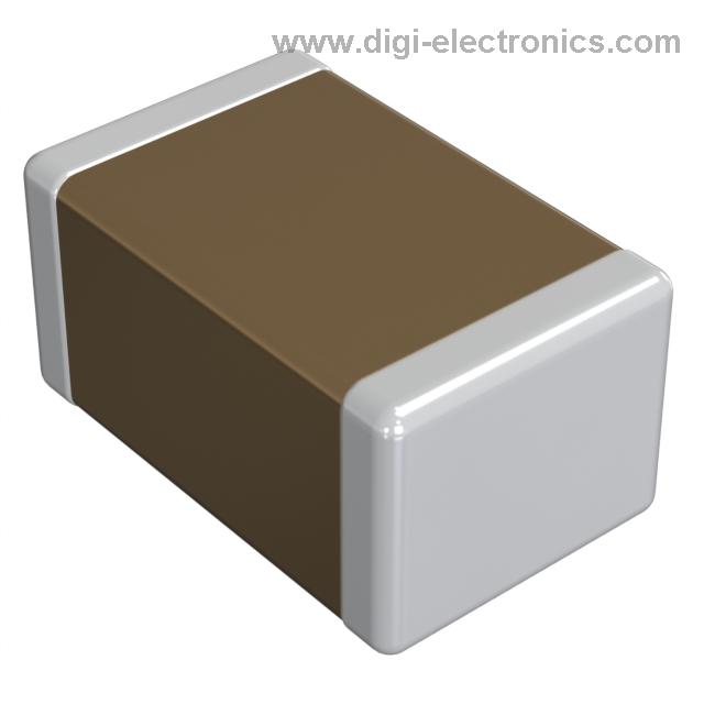
Product overview: GRM0335C1E8R2BA01D Murata chip ceramic capacitor
The GRM0335C1E8R2BA01D exemplifies Murata's innovation in multilayer chip ceramic capacitors, leveraging advanced C0G/NP0 dielectric technology to achieve remarkable temperature stability and precision. The dielectric material, fundamentally nonferroelectric, ensures negligible capacitance variation across a broad temperature range and low dissipation factor, which is instrumental for safeguarding signal integrity in frequency-sensitive environments. These properties become critical when integrated within RF front-end modules, impedance-matching networks, and precision oscillator circuits, where even marginal parameter drift can result in degraded system performance due to detuning or phase errors.
The 8.2 pF nominal value, paired with a strict ±0.1 pF tolerance, responds directly to the demands of compact, high-Q passive networks. Such precision not only simplifies simulation-accurate circuit modeling but also enables tighter production yield and reduced post-assembly adjustment. The 0201 (0603 metric) footprint further supports aggressive miniaturization in modern PCB layouts, contributing to reduced parasitic effects by minimizing pad and trace inductance. This granularity is crucial during RF design optimization, limiting unforeseen resonance and EMI susceptibility.
Murata's attention to surface-mount assembly compatibility manifests in both the terminations and the robust mechanical structure. Consistency during reflow soldering is achieved through reliable termination chemistry that resists degradation under thermal and chemical stress. Aspects like effective solder wetting and minimal tombstoning risk increase board-level reliability, which is especially valued during high-throughput assembly or miniaturized module integration where manual touch-up is unfeasible.
Within application scenarios, the GRM0335C1E8R2BA01D demonstrates its utility in VCO banks, precision filter poles, and input matching circuits, particularly where board real-estate constraints and the need for low-profile assemblies intersect. In high-frequency antenna matching, its stable capacitance under both bias and varied operational conditions translates to predictable impedance transforms, resulting in superior return loss and transmission efficiency. Designers can deploy these capacitors with confidence in tightly clustered circuit sections, where thermal gradients and mechanical strain may otherwise provoke parameter drift—this resilience stems from the NP0 composition and Murata’s established process control.
From a practical design perspective, maintaining consistent solder fillet and pad dimensions is essential to harness the intrinsic electrical performance, as any deviation can inadvertently introduce stray inductance or capacitance, degrading the intended response. This highlights the necessity of adhering to Murata’s recommended land pattern and reflow profiles during layout and assembly. Furthermore, in production environments emphasizing high-density placement, the 0201 size supports automated optical inspection and minimizes shadowing, allowing for streamlined quality verification.
The broader progression towards miniaturized passives, as represented by this device, signals a paradigm where greater emphasis is placed on component-level stability as a lever for system-level robustness. As integration density climbs, relying on devices such as the GRM0335C1E8R2BA01D enables circuit designers to push frequency, size, and consistency boundaries, directly influencing the downscaling of RF, timing, and analog signal chain architectures. This capacitor thus acts not only as a functional element, but as a strategic enabler for the evolution of next-generation electronic systems.
Technical specifications: GRM0335C1E8R2BA01D Murata performance & ratings
The GRM0335C1E8R2BA01D is a multilayer ceramic capacitor engineered for precision-critical applications, leveraging its C0G/NP0 dielectric to deliver exceptional temperature stability. This dielectric class maintains capacitance drift within 0 ±30 ppm/°C, upholding nearly invariant characteristics across a broad thermal spectrum. Such low drift is indispensable in RF topologies, oscillator frequency control, and analog filtering where even minor capacitance variations can induce phase errors, frequency shifts, or filter response anomalies.
Within its 8.2 pF nominal capacitance, tightly controlled to ±0.1 pF, the component suits high-frequency matching networks and impedance-tuned signal paths. The narrow tolerance is particularly relevant when cascading multiple passives, preventing cumulative error that might deteriorate signal integrity or system linearity. When allocated to timing circuits or clock lines in high-speed data environments, consistency across units simplifies circuit validation and accelerates design iteration cycles.
The 25V DC rated voltage accommodates a wide margin for signal excursions and power delivery, balancing size and reliability constraints present in advanced miniaturized PCBs. Engineers frequently encounter scenarios where compact placement imposes derating discipline, yet the GRM0335C1E8R2BA01D’s 0201 (0.6 x 0.3 mm) envelope allows for dense arraying in confined analog front ends and RF modules. Streamlining layouts at this scale can significantly reduce parasitic effects, boosting net system Q and facilitating predictable electromagnetic compliance results.
The device aligns with EIA standards for general purpose, high-stability multilayer ceramics, positioning it as a baseline for precision signal chains rather than bulk decoupling. Experience shows that integrating such capacitors into low-noise amplifier biasing or voltage-controlled oscillator tanks mitigates performance drift during both qualification and field operation. Selection of C0G/NP0 ceramics, despite marginally higher procurement costs or assembly overhead, often proves superior over X7R or Y5V alternatives by virtually eliminating temperature- and bias-induced tuning efforts.
Advanced applications—including fine-resolution analog-to-digital interfacing, RF filter bank realization, and high-Q resonator construction—leverage the component’s stability for predictable system performance over product lifespan. This approach reduces the engineering burden for periodic recalibration and yields measurable productivity gains during validation and compliance testing. Employing ultra-stable class I ceramics in such critical roles forms a resilient foundation for scalability and long-term maintainability across rapidly evolving electronic systems.
Application considerations: GRM0335C1E8R2BA01D Murata mounting, handling, and reliability
Mounting and handling of the GRM0335C1E8R2BA01D MLCC demand rigorous attention to stress factors that directly influence reliability and electrical stability. The direct surface-mount of this miniature capacitor on rigid or flexible substrates exposes the component to cumulative mechanical stress—particularly from PCB flexure, unwanted vibration, thermal gradients, and inadvertent mechanical impacts. In high-density designs, local board flex can create tensile and compressive forces at the chip terminations, risking micro-cracking of the dielectric or solder joint fractures, both of which greatly elevate leakage or catastrophic failure rates.
Critical layout discipline involves orienting the capacitor’s length parallel to the dominant flex direction whenever feasible, thereby distributing local stresses more evenly and reducing the risk of crack initiation at the ceramic body. Placement near stress-concentrating discontinuities—such as scored board edges, cutouts, or mounting holes—magnifies the probability of damage during assembly or service. It is advantageous to maintain generous keep-out zones around these features, particularly in miniaturized form-factor applications where board real estate is at a premium. Downstream processes, such as automated pick-and-place and reflow, require tightly controlled parameters. Gentle handling, careful nozzle pressure selection, and strict vibration damping protocols during transport significantly lower latent defect rates.
Temperature cycling, common in power and automotive electronics, imposes expansion mismatch between the chip body and substrate, often manifesting in internal microstructural defects. Selection of compatible PCB materials, combined with the use of soft-termination or flexible adhesive layers, can effectively interrupt crack propagation pathways and enhance operational endurance. Empirical analysis of site-specific stress patterns—using strain mapping or finite element modeling—unlocks the ability to adapt footprint geometries or reinforce critical regions proactively.
Functional fail-safety forms an essential pillar where insulation integrity is paramount. While short-circuit modes are relatively rare with proper assembly, their systemic consequences can be severe in high-reliability contexts. Protective circuit elements, such as series fuses or redundant parallel architectures, act as insurance layers, isolating faults to prevent cascade failures across sensitive loads. It is preferable to select fuse ratings that respond to expected MLCC short profiles, balancing coordination with overall protection strategy.
Iterative reliability improvement emerges from post-assembly inspection protocols and accelerated stress testing. High-resolution X-ray and micro-sectioning, when integrated into design validation, frequently reveal latent cracks or delamination not easily detected through routine visual checks. These empirical findings support continuous design adjustment, fostering a defect-averse hardware culture even as miniaturization trends push towards higher density and finer pitch.
The intersection of mechanical layout discipline, fail-safe design foresight, and data-driven process refinement defines a robust approach to GRM0335C1E8R2BA01D usage. By integrating mechanical and electrical perspectives into the design flow, engineers can ensure both the performance and field longevity of circuits leveraging compact, high-value MLCCs, maintaining operational integrity even under stringent deployment conditions.
Environmental and operational requirements: GRM0335C1E8R2BA01D Murata conditions and limits
The GRM0335C1E8R2BA01D capacitor from Murata is engineered for robust performance within tightly defined environmental and operational boundaries. The specified ambient range—temperature from +5°C to +40°C and relative humidity between 20% and 70%—reflects both the sensitivity of the ceramic dielectric and the susceptibility of silver-palladium or nickel electrodes to corrosion and oxidation. Extended storage outside these boundaries introduces risks, notably solderability degradation due to surface oxidation, and molecular-level instability of dielectric layers. Direct exposure to sunlight or corrosive gases accelerates aging and embrittlement, often leading to latent failures during reflow or operational stress.
Electrothermal management is paramount; the device’s total thermal load must consider not just ambient conditions but also self-heating driven by ripple and pulse currents. Excessive current induces localized temperature rises, which can shift material parameters and initiate microcracking—especially pronounced in multilayer ceramic architectures. A subtle but critical point is that the thermal gradient within a densely populated PCB region may diverge from bulk ambient readings; thus, thermal simulation and real-time sensing should be integrated during prototyping to avoid cumulative deviation past the 40°C upper bound.
Voltage derating is non-negotiable. Operating the capacitor at or above its rated 2V can trigger non-linear dielectric responses, dielectric breakdown paths, and eventual catastrophic short-circuits. In systems with analog timing or filtering roles, voltage and temperature transients must be scrupulously modeled. Capacitance drift stems from intrinsic material aging and extrinsic stressors; it follows a log-linear decay profile, usually exacerbated by thermal cycling. In dynamic environments, like precision oscillators or coupling applications, a best practice is periodic impedance and value characterization, confirming stable electrical performance. Board-level validation with in-circuit diagnostics routinely identifies early deviations—an approach that minimizes field returns.
Implementation wisdom suggests proactive moisture control, such as desiccant-packed storage or nitrogen-purged cabinets for ultra-miniature types like the GRM0335C1E8R2BA01D. Cleaning and assembly steps should exclude halogenated fluxes and aggressive washes, as residues elevate corrosion risk. Board layout should account for localized heating and stray EM fields, leveraging ground planes and thermal reliefs to attenuate unwanted coupling and ensure thermal uniformity. Model-based design, backed by empirical data from accelerated life testing, enables predictive failure analysis and long-term reliability assurance.
In summary, the intersection of environmental controls, electrical derating, and ongoing validation forms a proven workflow for maximizing service life. The nuanced interplay between ambient chemistry and physical stress requires continuous optimization at both design and production stages, underlining the criticality of embedded sensing and predictive analytics in next-generation electronic assemblies.
Soldering and board assembly: GRM0335C1E8R2BA01D Murata process guidelines
Soldering and board assembly processes for the GRM0335C1E8R2BA01D Murata multilayer ceramic capacitor demand strict process control to ensure SMT reliability and long-term device integrity. Precise thermal management forms the foundation of high-yield production. During reflow and wave soldering, the temperature profile must be tightly regulated. Gradual ramp-up minimizes thermal gradients, which, if abrupt, can induce microcracks or delamination within the capacitor structure. Optimal preheat cycles help maintain uniform board and component temperatures, particularly critical for 0201-size chips where mass differences quickly translate into uneven heat stress.
Solder application requires calibrated volumes. Excess solder increases thermal and mechanical stress at terminations, promoting chip cracking or early failure under vibration or thermal cycling conditions. Insufficient solder—often the result of underspecified paste deposition or misaligned stencil apertures—compromises joint adhesion and electrical contact, exposing the assembly to open-circuit risks. Systematic monitoring of solder fillet geometry during process validation stages can preempt stress-related incidents and ensure robust electrical connections.
Rework presents inherent risk to miniature MLCCs. The application of excessive heat, especially without prior component preheating, can exacerbate mechanical shock and encourage internal electrode migration or dielectric breakdown. A controlled approach limits direct soldering iron contact and prioritizes thermal uniformity. The selection of adhesives and fluxes further impacts microstructure reliability. Avoiding aggressive chemistries—such as strongly acidic or water-based fluxes—protects against premature oxidation and internal corrosion, key factors in long-term reliability for high-density boards.
Equipment calibration emerges as a decisive factor in preventing placement-induced damage. Pick-and-place machinery must be regularly maintained to sustain force thresholds compatible with fragile ceramic bodies. Misalignment or excessive downward pressure during high-speed placement can induce chipping that escapes standard visual inspection but becomes manifest during subsequent electrical test or field deployment. Implementation of in-line AOI for real-time defect detection forms a powerful safeguard in volume production environments.
Post-solder cleaning routines demand solvent compatibility testing and ultrasonic exposure controls. Energetic ultrasonic cleaning is capable of fracturing the capacitor’s ceramic matrix or undermining termination integrity. Selection of cleaning agents shouldn’t solely optimize flux removal rates; their ionic compatibility with board substrates and MLCC materials must be verified to safeguard against latent electrical drift or corrosion under bias conditions. Process engineers have found comprehensive batch validation and periodic ion chromatography analyses effective in benchmarking cleaning process reliability against rising miniaturization trends.
A remarkable trend is emerging toward predictive process control, leveraging real-time thermal simulation and automated vision inspection to fine-tune every SMT stage for miniature components like the GRM0335C1E8R2BA01D. This integration of digital process monitoring and feedback loops not only prevents classic physical defects but also enables continuous improvement of assembly line yields—validating that microelectronic reliability increasingly depends on holistic, tightly interconnected process discipline rather than on isolated procedural compliance.
Packaging and storage: GRM0335C1E8R2BA01D Murata logistics best practices
Packaging and storage of Murata’s GRM0335C1E8R2BA01D multilayer ceramic capacitors pivot on both mechanical precision and environmental control to safeguard device reliability. The tape-and-reel carriers are engineered to maintain precise component orientation, minimizing the risk of mechanical stress during automated mounting processes. Carrier tapes are specified with tight tolerances in pocket dimensions, material rigidity, and cover tape adhesion—a control loop that avoids both displacement and excess retention force, which are frequent culprits of stress-induced cracking. During packaging, electrostatic discharge (ESD) safeguards are embedded in process flow, as even marginal ESD events can initiate latent degradation not immediately evident during in-circuit tests.
Material handling protocols are explicitly oriented around preservation of the ceramic’s microstructure. The sealed packaging serves as a primary barrier against the ingress of moisture and corrosive gases, especially chlorine- or sulfur-containing volatiles that accelerate electrode oxidation. This barrier function supports a controlled storage microclimate where temperature must remain between 5°C and 40°C, and relative humidity below 60%. Exceeding these windows promotes hydrolysis or electrode migration, undermining reliability parameters such as insulation resistance and ESR. Time-in-storage limits (typically six months) are not arbitrary; they are defined by empirical Arrhenius modeling correlating ambient conditions with diffusion rates and interfacial reactions at the terminations. This quantification enables predictive maintenance schedules and batch-level risk scoring in inventory management systems.
Transportation logistics further demand multi-axis shock and vibration isolation. Mechanical shocks above specified G-ratings or repetitive vibration sequences can propagate microcracks within the dielectric layers, generating sites for catastrophic shorting under voltage bias. Impact events may leave no outward trace yet precipitate subsequent failures as thermal and electrical cycling accentuate these sub-visible defects. Protective intermediate packaging with multi-layered cushioning, coupled with the use of drop sensors and data loggers, facilitates traceability and rapid root-cause analysis in the event of out-of-spec arrivals.
Effective deployment in high-reliability assemblies requires docking product usage with real-time environmental monitoring and first-in, first-out (FIFO) inventory strategies, ensuring exposure times and conditions do not breach thresholds. Removing components from sealed packaging only immediately before production mitigates surface adsorption of moisture, which can otherwise amplify thermo-mechanical mismatch stress during soldering. The value of segregated storage—physically isolating high-spec MLCCs from other goods prone to off-gassing or particulate generation—often emerges only after anomalous field failures are traced back to cross-contamination, highlighting the non-trivial linkage between logistics discipline and field performance statistics.
At the system level, integrating transport and storage data into product lifecycle management platforms supports predictive analytics for supply-chain resilience, enabling rapid intervention when real-world conditions deviate from prescribed models. This approach, embedding logistics constraints into routine production and risk management, elevates MLCC reliability from a component-level attribute to a supply-chain quality differentiator. Through such multi-layered process coherence, organizations bypass typical pitfalls that compromise ceramic capacitor integrity, achieving both operational continuity and robustness in end-use environments.
Potential equivalent/replacement models: GRM0335C1E8R2BA01D Murata alternatives in engineering
In the context of high-frequency applications, careful component selection is critical when considering replacements for capacitors such as the GRM0335C1E8R2BA01D from Murata. Evaluation must prioritize key electrical parameters. Capacitance value at 8.2 pF and a minimum voltage rating of 25V represent the initial screening criteria, ensuring direct circuit substitution without compromise of signal integrity.
Equally pivotal is the dielectric classification; the use of C0G/NP0 ceramics is essential owing to their minimal temperature coefficient and excellent aging performance. This stability across temperatures and time directly translates to reliable performance within RF modules and high-speed analog signal chains. Small deviations in these parameters can degrade circuit Q-factor or introduce phase noise, especially where tolerances are tightly controlled. Consequently, practical substitution efforts entail reviewing technical datasheets for nuances in tolerance, temperature drift, and specified aging rates—the latter often overlooked but critical for precision designs.
Form factor plays an instrumental role, with the 0201 (metric 0603) footprint presenting challenges both for soldering process control and for electrical parasitics. In high-density layouts, even minor discrepancies in mounting or terminations can alter PCB impedance profiles. Experienced practitioners routinely confirm mechanical and solderability parameters using sample lots before full-scale production, mitigating risks of reflow anomalies or pick-and-place issues.
Product cross-referencing requires more than superficial part number matching. Murata’s comprehensive documentation allows for direct mapping across the GRM series, but cross-vendor comparison—such as to TDK or Samsung Electro-Mechanics variants—demands granular review of equivalent series resistance (ESR) and self-resonant frequency, particularly for RF and impedance-matching circuits. Automated tools facilitate initial screening, but hands-on evaluation under actual operating frequencies often exposes edge-case discrepancies.
A key insight is that “equivalent” listed in supplier cross-reference tables often refers only to headline specifications. Application engineers rely on bench characterization and pre-qualification cycles to validate signal integrity impacts, especially for designs subject to environmental stresses or performance certification. This empirical diligence underlines the importance of not only electrical and mechanical congruence, but also a deep technical appreciation for application expectations when selecting and qualifying alternatives.
Conclusion
The GRM0335C1E8R2BA01D Murata capacitor exemplifies the advantages of C0G/NP0 class ceramics, offering a stable capacitance over wide temperature and voltage ranges. In advanced analog and RF circuits, fluctuations in capacitance directly translate to signal drift and impedance mismatch. The C0G/NP0 dielectric deployed here exhibits minimal temperature coefficient and negligible piezoelectric noise, mitigating phase errors and jitter in timing circuits as well as distortion in signal paths. The inherent material properties enable designs that demand sub-picofarad precision for filter networks, oscillator arrays, and impedance-matching blocks.
Miniaturization remains a persistent challenge in board design, particularly with rising system densities. The 0201 footprint of this component facilitates tight placement in constrained geometries typical of modern multi-layer PCBs. This scaling, however, necessitates disciplined handling during assembly. The capacitor’s small mass and leads increase vulnerability to thermal and mechanical stress during reflow soldering. Experience shows a direct link between solder joint quality and device reliability; best practice mandates controlled reflow profiles and minimized physical manipulation post-placement. Automated pick-and-place equipment calibrated for micro-sized passives can improve yield, with periodic inspection cycles identifying latent mounting issues early in the process.
Operational integrity must be sustained across diverse ambient conditions. The C0G/NP0 technology enables continuous function even with large swings in humidity or high-frequency pulsing, contributing to long-term drift rates that are markedly low. Comparative evaluation against alternative dielectrics such as X7R or Y5V reveals significant performance stability advantages for timing and RF-centric domains. For applications in wireless modules, low-noise amplifiers, and clock distribution matrices, this characteristic translates to greater circuit margin and more predictable aging.
Bill of Materials optimization extends beyond mere parameter matching. Cross-referencing equivalent models from other manufacturers—while factoring dielectric class, tolerance band, and thermal profile—supports risk mitigation and multi-source procurement strategies. Subtle design tweaks, like selecting slightly tighter tolerance bins or rebalancing layout to accommodate the smaller footprint, can compound gains in reliability and long-term service support. Evaluating supply chain consistency and lifecycle guarantees complements the technical assessment, especially for platforms intended for extended deployments.
An overarching insight emerges from multi-generational product integration: precision ceramic capacitors, such as the GRM0335C1E8R2BA01D, profoundly affect the signal fidelity and operational envelope of analog and RF circuits. Diligent process control, targeted material selection, and contextual application knowledge together leverage the full capabilities of this class, often forming the backbone of robust high-performance electronic design.


