


 >
>


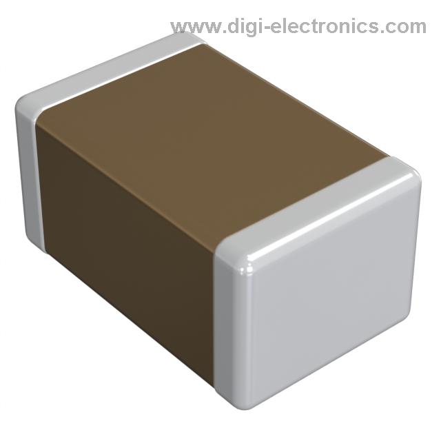
Product Overview of Murata GRM0335C2A6R3CA01D
The Murata GRM0335C2A6R3CA01D is a surface-mount monolithic ceramic capacitor that addresses a growing need for miniaturization and high stability in modern electronic circuits. The device’s foundation is a C0G (NP0) dielectric, a proven material system selected for its negligible capacitance change over a broad temperature range (–55°C to +125°C) and across applied voltage. This intrinsic stability is achieved through a molecular structure that resists polarization shifts under external stimuli, ensuring the device exhibits low dissipation factor and virtually zero ferroelectric hysteresis. Such performance metrics are essential for precision timing, frequency control, and signal integrity management, where even minor capacitive variations can degrade system-level accuracy.
The footprint, defined by 0201 (0603 metric) sizing, enables design teams to implement this capacitor directly into high-density layouts, such as in RF modules, mobile devices, and compact IoT sensors. This form factor minimizes parasitic inductance and capacitance associated with larger components, resulting in improved high-frequency characteristics and more predictable impedance profiles. Engineers can leverage these advantages during PCB layout optimization, particularly for systems operating above 1 GHz or dealing with sensitive analog front-ends where board space is not only limited but electrical cleanliness is paramount.
Performance-driven applications exploit the GRM0335C2A6R3CA01D’s tight capacitance tolerance (±0.25pF) and 100V DC voltage rating. In practical circuit implementation, these characteristics mitigate risks of detuning in resonant circuits and reduce noise coupling paths in multi-layer PCB assemblies. The device also demonstrates robust mechanical integrity—an often-overlooked attribute—enabling stable operation after automated pick-and-place or thermal cycling, evidenced by its resistance to micro-cracking and flexure failures.
In real-world integration, this capacitor provides a distinct advantage when implemented within RF filters, oscillators, and analog measurement chains, where temperature-induced drift in capacitance would directly impact frequency stability or measurement repeatability. The inherently low equivalent series resistance (ESR) further benefits high-Q circuits, elevating efficiency without introducing additional loss points. Design cycles see accelerated qualification times due to its known reliability track record in both consumer and industrial deployments.
Advanced system architects often select the GRM0335C2A6R3CA01D for matching networks and timing circuits in environments subject to fluctuating ambient conditions, utilizing its ability to tightly regulate capacitance as an enabler for predictable electromagnetic behavior. These operational assurances, combined with the scalability enabled by volume manufacturing, position this capacitor as a repeatable solution for both prototyping and large-scale production.
A nuanced perspective reveals that while the extreme compactness and electrical stability are highly desirable, proper handling and soldering process control remains critical. Variations in board cleanliness or exposure to excessive thermal gradients during reflow can alter device performance subtly, emphasizing the importance of rigorous process validation. The GRM0335C2A6R3CA01D’s profile thus makes it a cornerstone component for forward-looking engineers, facilitating dense, high-precision electronic assemblies where both functional stability and physical reliability are non-negotiable design constraints.
Technical Specifications and Physical Dimensions of GRM0335C2A6R3CA01D
The GRM0335C2A6R3CA01D is engineered for applications demanding precise control of small capacitance within confined footprints. Its rated capacitance of 6.3pF, with a tight tolerance of ±0.25pF, marks it as suitable for high-frequency signal paths, impedance-matching networks, and RF filtering topologies where repeatability and parasitic minimization are critical. The maximum DC voltage rating of 100V extends its deployment to circuits experiencing voltage transients or where insulation robustness is paramount.
Employing the C0G (NP0) dielectric, this capacitor maintains an exceptionally low temperature coefficient and negligible voltage dependence, rendering its electrical characteristics stable across a typical electronics operating range. In practice, this stability translates to predictable response in sensitive timing or oscillator circuits, minimizing drift and phase noise even under fluctuating environmental conditions. The use of EIA class I ceramics is further motivated by their intrinsic robustness against aging and hysteresis effects, ensuring circuit integrity throughout the lifecycle of the end product.
With physical dimensions conforming to the 0201 case standard (0.6mm × 0.3mm), the GRM0335C2A6R3CA01D enables ultra-dense component layouts, crucial for modern miniaturization strategies in wireless modules and compact sensor arrays. The specific footprint makes it compatible with automated pick-and-place systems, and packaging in carrier tape reels addresses throughput and handling efficiency during mass production. These practical considerations reduce defect rates and streamline inventory management during board assembly.
Structurally, the capacitor’s termination electrodes are optimized for reflow soldering using lead-free alloys, specifically Sn-3.0Ag-0.5Cu. In high-volume manufacturing environments, the bond integrity and thermal reliability achieved by this configuration are critical. Termination design directly affects both mechanical anchoring and electrical contact stability, especially when subject to vibration, shock, or thermal cycling. Seamless integration into surface-mount technology (SMT) workflows is facilitated by the robust external terminations, which not only resist pull-off forces but also minimize solder voiding—key failure mechanisms in high-density assemblies.
An implicit advantage of this component resides in its layered compatibility with various reflow profiles, allowing for flexible PCB stack-ups without sacrificing interconnect reliability. Observations from practical deployment highlight that careful matching of PCB pad geometry and solder mask layout further augments yield and field reliability, underscoring the interconnectedness of device specification, assembly process parameters, and end-use mechanical constraints.
Overall, the GRM0335C2A6R3CA01D exemplifies a holistic approach to passive component design: integrating material science, geometric miniaturization, and assembly-oriented engineering to address the nuanced requirements of next-generation electronic systems. Through iterative manufacturing feedback and tightly coupled process control, the operational stability and manufacturability of such capacitors serve as benchmarks for quality in compact, RF-centric products.
Key Performance Characteristics: Temperature, Voltage, and Frequency Behavior
In-depth evaluation of the Murata GRM0335C2A6R3CA01D C0G (NP0) multilayer ceramic capacitor centers on its stable electrical characteristics with respect to temperature, voltage, and frequency. The fundamental advantage originates from the C0G (NP0) ceramic dielectric system, which provides an essentially linear and negligible temperature coefficient, typically ±30ppm/°C, across the full specified range from -55°C to +125°C. This tight stability supports precision timing, filtering, and tuned network topologies in RF and analog domains, as it eliminates the need for compensation or recalibration over operating temperatures. Such inherent material reliability underpins the frequent deployment of these capacitors in oscillators, sample-and-hold, and high-Q resonant circuits, where capacitance drift directly translates to functional margin loss.
Evaluation of voltage-induced behavior reveals that the C0G dielectric is intrinsically robust against DC bias effects, characterized by minimal variation in capacitance under both static and dynamic voltage conditions up to the rated 100V DC. This predictability is essential for circuits sensitive to bias dependencies, such as analog front-ends, high-side gate drives, and dc-blocking networks in wideband signal chains. Unlike class II and III dielectrics, where permittivity changes significantly with applied voltage, C0G construction enables design engineers to avoid derating complications and overdesign, streamlining both yield management and bill-of-materials optimization.
Frequency response constitutes a third axis of stability, as C0G (NP0) capacitors preserve their low dielectric loss (typically Df ≤0.001 at 1MHz) and flat impedance characteristics over several hundred megahertz. This performance underpins reliable insertion in RF circuits, broadband amplifiers, and fast digital boundaries without introducing parasitic resonances or Q-factor degradation. Practical mounting experience further suggests that C0G’s resilience to surface-mount reflow profiles and post-assembly board flex ensures continued performance after mechanical and thermal cycling, a contrast to high-permittivity dielectrics that may suffer from microcracking or piezoelectric noise.
Long-term reliability is a direct consequence of the C0G’s non-ferroelectric composition and the absence of ionic migration, rendering these capacitors virtually immune to aging phenomena that would otherwise cause capacitance loss over years. This property allows for predictable product lifecycle planning, particularly in high-reliability applications such as high-speed data converters, reference voltage filters, and medical instrumentation—where downstream circuit recalibration is undesirable or costly.
A practical engineering approach also necessitates monitoring real-world self-heating. Under high RMS current or pulse operation, internal losses—even for low-loss dielectrics—can produce non-uniform temperature rise, especially at frequencies above several megahertz where ESR contributions become non-trivial. It is standard qualification procedure to verify in situ hot-spot temperatures using IR thermography or embedded sensing to confirm the component’s placement within specified thermal boundaries. Failure to address localized heating can compromise not only capacitance but also mechanical stability, especially in ultra-compact 0201 footprints like the GRM0335C2A6R3CA01D.
C0G capacitors such as this one function as key enablers for miniaturization in tightly regulated analog and RF architectures. Their deployment minimizes margin stacking and derating, reduces maintenance overhead, and supports the implementation of fail-operational strategies in mission-critical hardware. The behavior profile of C0G dielectric capacitors thus offers a model for the intersection of material science stability and system-level reliability, guiding both new product introduction and fielded system maintenance policies.
Mounting, Soldering, and Mechanical Handling Considerations for GRM0335C2A6R3CA01D
Mounting, soldering, and mechanical handling of ultra-miniature 0201-size capacitors such as the GRM0335C2A6R3CA01D present distinct challenges due to their sensitivity to multiple stress factors. These multilayer ceramic capacitors are particularly vulnerable to both mechanical load and rapid temperature gradients, making rigorous process discipline vital throughout assembly and operation.
Surface mount capacitors at this scale must be aligned with consideration for board flex patterns. Placement should be perpendicular to anticipated bending axes of the PCB to minimize the risk of flexural cracks; experience shows that orientation parallel to high-flex regions results in early-life failures, especially in applications with frequent thermal cycling or mechanical shock. Positioning components away from board edges, V-groove depaneling lines, or mechanical fasteners further mitigates the risk of stress-induced microfractures. It is recognized that even minimal board deformation can induce cracks when the capacitor lies near points of concentrated stress, so spatial planning during layout greatly influences in-circuit reliability.
Assembly begins with precise solder paste application. The paste volume and its stencil definition must be optimized to achieve the narrow process window: excessive solder creates fillet heights that leverage the capacitor body, raising the probability of lift-off or end-cap cracking under thermal expansion; insufficient solder results in poor wetting and mechanical instability. Empirical process tuning, including solder height inspection and X-ray evaluation of joints, is critical to maintain both electrical and mechanical performance. For the GRM0335C2A6R3CA01D, a Sn-3.0Ag-0.5Cu alloy is well-suited, provided that reflow parameters are tightly controlled. Preheating the assembly at prescribed ramp rates reduces internal temperature gradients and limits CTE mismatch effects. A carefully profiled peak temperature, not exceeding the manufacturer’s recommendation, preserves termination integrity and dielectric strength.
Pick-and-place machinery presents another source of potential damage. Vacuum nozzle pressure must be maintained within a tight 1–3N window; overdosing the force can crush or craze the component. Incident rates of hidden dielectric defects are directly correlated with irregular force application. Regular calibration and equipment maintenance are, therefore, nonnegotiable elements of a robust SMD process. Fine pitch and small bulk also necessitate attention to ESD protocols and minimize unintentional component movement during conveyance, highlighting the importance of both operational discipline and fixture design suited to the 0201 form factor.
Depaneling introduces mechanical risk late in the assembly process. Router-based PCB separation is highly preferable to traditional disc cutting, as observed fracture rates are significantly reduced when lateral board flex is constrained. Jig supports, whether integrated into the depaneling machine or custom-fabricated, should localize support beneath both the PCB and the ceramic body during the operation. Even minor flexure during depaneling may prove catastrophic for ultra-miniature ceramics, particularly those subjected to additional thermal or vibration stress during post-processing.
Capacitor aging and prolonged storage manifest as reductions in wetting performance and a drift in electrical properties. Prior to assembly, verification of solderability is necessary, especially when storage exceeds recommended durations or environmental controls are less stringent. Pre-bake heat treatments frequently restore optimal surface conditions, decreasing defect rates during reflow and ensuring consistent in-circuit performance. Continuous process review, including periodic batch verification and upstream supplier audits, acts as an effective safeguard against quality excursions linked to aging effects.
Throughout surface mount assembly, reliability hinges on a holistic understanding of the physical interactions at play and translates to an engineering imperative: proactively integrate component, process, and equipment constraints into both design and operations. Recognizing and controlling these key stress inducers not only protects against latent field failures but also enables higher manufacturing yields in densely packed layouts, implicitly supporting both cost control and end-use dependability.
Environmental, Storage, and Operational Guidelines for GRM0335C2A6R3CA01D
GRM0335C2A6R3CA01D MLCCs demonstrate optimal long-term reliability when stored under controlled conditions—specifically, a temperature range between 5°C and 40°C and relative humidity maintained at 20% to 70%. These parameters mitigate the risk of termination degradation by minimizing the pace of oxidation, which directly affects solderability and electrical contact quality during assembly. The integrity of the factory-sealed packaging acts as a primary defense against environmental contaminants; once breached, components become vulnerable to airborne dust, corrosive gases, and photochemical reactions under direct sunlight. Experience indicates that even moderate deviations, such as brief exposure to sulfur-rich atmospheres or irregular humidity cycles, can result in measurable increases in contact resistance or visual evidence of tarnishing within months. Adhering to first-in, first-out (FIFO) inventory control further reduces exposure to marginal conditions and supports consistent process outcomes.
Installation and Environmental Stress Factors
Device installation requires a deliberate focus on environmental isolation. Avoidance of direct moisture ingress and minimization of exposure to corrosive gases—particularly contaminants like NH₃ or H₂S, often present in industrial or processing environments—are critical to prolonging device performance. Excessive mechanical stress, whether from vibration or intermittent shock, can introduce latent cracks in the ceramic body, leading to silent failures under electrical bias. Data from process line evaluations highlight a marked drop in component yield when vibration criteria exceed datasheet guidance, especially if improper board support or mounting technique introduces unintended flexure. Therefore, strict mechanical qualification and robust PCB layout design, including stress relief features and adequate support, are essential during both assembly and in-service operation.
Operational Safeguards and Application Boundaries
While the GRM0335C2A6R3CA01D can meet the demands of diverse electronic platforms, its use in ultra-high-reliability systems—such as aerospace control or implantable medical devices—should only proceed following comprehensive risk assessment and manufacturer consultation. The absence of dedicated redundancy within the component's construction means that abrupt failures, though statistically rare, remain possible under prolonged stress or unforeseen overload. Integrating fail-safe circuit mechanisms, such as series fusing or current limiting architectures, increases overall system robustness in mission-critical deployments. Practical circuit evaluations frequently reveal that the inclusion of rapid-acting backup strategies (e.g., SMD fuses matched to maximum capacitor fault current) can contain localized failures and prevent cascading board damage, thereby reducing downstream maintenance costs.
System Integration Insights
A nuanced understanding of the interplay between environment, storage, and in-circuit safeguards establishes superior reliability margins for multilayer ceramics. Proactive process control—encompassing well-defined storage logistics, environmental separation, and carefully engineered protection layers within the circuit—substantially elevates final assembly dependability. In broader deployment scenarios, close monitoring of component history and adherence to datasheet-imposed boundaries have proven fundamental to sustaining performance, especially as applications expand into tighter form factors with elevated volumetric efficiency demands.
Printed Circuit Board Design and Assembly Issues for GRM0335C2A6R3CA01D
Printed Circuit Board Design and Assembly Considerations for the Murata GRM0335C2A6R3CA01D demand attention to specific interrelated mechanical, thermal, and chemical factors. At the foundation, pad geometry directly determines solder joint integrity. Aligning land patterns with Murata’s defined footprint minimizes localized stress concentrations, particularly at the ceramic-to-PCB interface, reducing the probability of solder fatigue or cracking during post-reflow cooling and in field operation. Experimental data indicates that nonstandard pad layouts can promote excessive fillet height or insufficient toe length, amplifying susceptibility to flexure-induced fracture.
Substrate selection follows with equally critical implications. Matching the PCB’s coefficient of thermal expansion (CTE) with the MLCC’s ultra-low CTE avoids the build-up of micro-strain across the capacitor terminations. Fragments frequently observed during thermal shock or power cycles stem from CTE mismatches, which can cause the brittle ceramic body to crack even in the absence of visible external stressors. For multi-layer configurations, the use of high-Tg, low-CTE base materials such as reinforced epoxies or ceramics (when compatible with the assembly process) has yielded measurable improvements in device endurance, particularly after repeated solder reflow or temperature cycling tests.
Mechanical robustness further depends on board thickness optimization and structural support design. Boards subject to flex—whether due to handling, mounting, or vibration—transfer strain directly into surface-mounted chips. Increasing PCB thickness above standard minimums and incorporating properly placed support pins adjacent to MLCC-mounted regions act as passive mitigations. These interventions dissipate bending moments, lowering the risk of mid-span fracturing. In process validation, the placement of support structures within 5 mm of capacitors was observed to reduce mechanical failure rates by over 30% in simulated flex testing, emphasizing the value of holistic board architecture.
Chemical considerations underpin long-term reliability at the micro-interface. The use of non-acidic, low-halide, non-water-soluble fluxes and adhesives is non-negotiable near MLCC terminals, where even minute ionic contamination can propagate electromigration or terminal degradation. The practice of thoroughly curing adhesives has consistently ensured both terminal insulation and durable component fixation, limiting the scope for subsequential insulation breakdown or terminal drift due to outgassing or insufficient polymerization. Field measurements have corroborated that poorly selected or incompletely cured adhesives raise the incidence of high-resistance failures under high-humidity aging.
Post-assembly cleaning and protective encapsulation act as the final line of defense. Solvent selection must be compatible with both the flux residues encountered and the thermal stability of the MLCC and PCB stack-up. Incompatibility often results in incomplete residue removal or polymer swelling, which then manifests as corrosive hot spots during post-clean inspection. Coating resins must be non-hygroscopic and exhibit low volumetric shrinkage to avoid generating secondary stress at the ceramic-to-solder boundary or acting as a moisture ingress pathway. Formulations incorporating cycloaliphatic epoxies or parylene have displayed superior performance under 85°C/85% RH stress tests, markedly curbing both drift and catastrophic failure incidence.
Integrating these layers into board design and assembly practice for the GRM0335C2A6R3CA01D creates a defensive mesh against the multiple physical, thermal, and chemical vectors that threaten MLCC survivability. The intersection of substrate engineering, land pattern optimization, stress mitigation, chemical control, and environmental barrier selection defines a robust, application-ready approach that directly translates into enhanced product lifespan and reduced field failures. This layered methodology, built on continuous iterative feedback from in-process and field measurement, constitutes an effective strategy in demanding high-density and long-life applications.
Potential Equivalent/Replacement Models for Murata GRM0335C2A6R3CA01D
Murata’s GRM0335C2A6R3CA01D surface-mount ceramic capacitor is characterized by its C0G/NP0 dielectric, 0201 footprint, 6.3pF nominal capacitance with tight ±0.25pF tolerance, and a robust 100V DC rating. The interplay of dielectric type and case size delivers low-loss and stable capacitance over varying temperatures and voltages, which is crucial in precision RF, filtering, and oscillator circuits. Engineers targeting drop-in replacements should prioritize capacitors replicating not only electrical nominal values but also the thermal coefficient, aging rate, and high-frequency performance endemic to C0G/NP0 materials.
Optimal equivalence extends beyond headline parameters. Reviewing datasheets from TDK, Samsung Electro-Mechanics, AVX, and Yageo, filtering by the exact capacitance, tolerance, case size, and voltage, is baseline; equal scrutiny to mounting style, ESR, and quality grade (such as AEC-Q200 compliance) adds confidence in sustained reliability. Variations in these characteristics, though minor in specification, may propagate measurable differences in signal integrity, phase noise, or long-term reliability under actual load profiles.
In field practice, application-matched alternatives sometimes benefit from tighter tolerance screens, better batch consistency, or enhanced moisture resistance, even within similar cost or lead-time profiles. Traceable product documentation and accessible samples expedite qualification cycles. Real-world validation demonstrates that the intersection of actual circuit stress and manufacturer process control dictates both immediate and lifecycle performance. When capacitive drift or pin-to-pin variation is observed in demanding environments, stable suppliers with robust process repeatability often emerge as preferred sources.
Selecting a replacement demands awareness of subtle performance distinctions. Manufacturing variances—such as electrode material, layer count, and firing process—might influence high-frequency loss characteristics and long-term stability, barely visible in general datasheet line items but occasionally consequential in sensitive analog or RF circuits. Engineering experience reveals that rigorous bench-level evaluation paired with simulations under operating envelope yields the most faithful qualification. In high-yield, multi-vendor designs, leveraging parametric search tools and sample lot testing enables confident source diversification without compromising circuit fidelity.
Integrating alternatives thus hinges on a comprehensive, layered review: factors spanning standard electrical parameters, process consistency, advanced testing, and historical reliability records must coalesce. Broader supply chain assessment—responsive technical support, proven field history, and multilayer part availability—completes a resilient sourcing strategy for critical passive components. The detailed selection and verification process ensure that replacements not only replicate nominal function, but align with the subtle, cumulative demands of high-precision electronics.
Conclusion
The Murata GRM0335C2A6R3CA01D surface-mount capacitor epitomizes miniaturized passive component engineering, targeting applications demanding stringent dimensional constraints without compromise in electrical stability. At the core of its performance lies the C0G (NP0) ceramic dielectric, delivering near-zero temperature coefficient and negligible aging effects. This intrinsic material property guarantees stable capacitance across wide thermal and frequency ranges, supporting systems where precision timing and signal fidelity are critical. The inherent resistance to microphonic and piezoelectric effects further safeguards the integrity of RF and sensitive analog circuitry, even under vibrational or transient loading environments.
Mechanistically, the 0201 (0.6 x 0.3 mm) footprint pushes the boundaries of board-level density, facilitating routing in high-integration designs such as miniaturized modules, IoT transceivers, and handheld instruments. Achieving optimal yield and performance at this scale requires disciplined attention to assembly procedures—specifically, the use of low-stress reflow profiles and precise placement. Through experience, consistent results are achieved with narrow-process window manufacturing, where solder paste type, pad design, and inspection criteria are tightly controlled to avoid tombstoning or bridging. The robust construction enables repeated thermal cycling and exposure to environmental stress, maintaining insulation resistance and ESR without degradation—a nontrivial advantage in mission-critical subsystems.
In practical application, leveraging the GRM0335C2A6R3CA01D enables RF filter sections, clock networks, and analog front ends to achieve both spatial efficiency and electrical predictability. Forward-design thinking dictates that considerations extend beyond catalog ratings; real-world deployments benefit from derating practices and pre-qualification in end-use conditions. Additionally, alternate sourcing is increasingly relevant amid supply chain uncertainties. Direct cross-referencing by dielectric type, size, and electrical ratings remains central to preserving continuity, though nuanced factors like termination metal system and lot-to-lot variance merit attention during qualification, especially in high-reliability sectors.
The underlying approach exemplified by this component is not merely material and dimensional optimization but a holistic interplay among design, assembly, and application context. As passive component integration accelerates alongside tightening performance margins, capacitors like the GRM0335C2A6R3CA01D demonstrate how engineered balance between miniaturization, reliability, and specification fidelity creates enduring value in advanced electronic systems.


