Counterfeit and defect prevention

Visual and packaging inspection

Electrical performance verification


 Clear All Products
 >
>


365 - Day Quality Guarantee - Every part fully backed.
90 - Day Refund or Exchange - Defective parts? No hassle.
Limited Stock, Order Now - Get reliable parts without worry.
Worldwide Delivery in 3-5 Business Days
100% ESD Anti-Static Packaging
Real-Time Tracking for Every Order


Credit Card, VISA, MasterCard, PayPal, Western Union, Telegraphic Transfer(T/T) and more
All payments encrypted for security


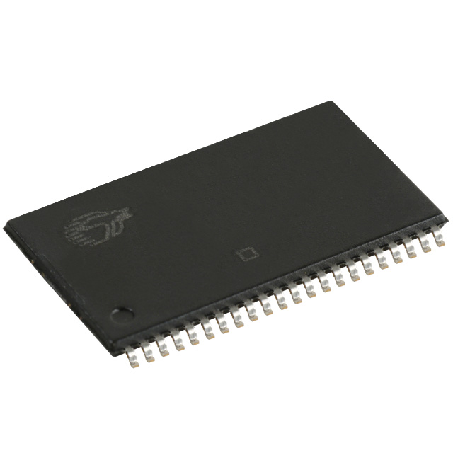
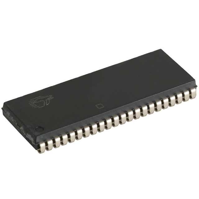
CY62146G30-45ZSXA-DG
DiGi ensures the quality and authenticity of every electronic component through professional inspections and batch sampling, guaranteeing reliable sourcing, stable performance, and compliance with technical specifications, helping customers reduce supply chain risks and confidently use components in production.


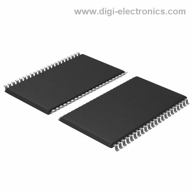
 Infineon Technologies CY62146G30-45ZSXA PCB symbols & footprints