 >
>


Product overview of EFM32WG942F256-B-QFP64
The EFM32WG942F256-B-QFP64 integrates a 32-bit ARM Cortex-M4F core, facilitating digital signal processing and floating point operations with hardware acceleration. This combination significantly enhances real-time control responsiveness and data throughput while maintaining precision in computation-heavy workloads. Operating speeds reach up to 48 MHz, positioning the device as an optimal choice for scenarios where deterministic timing and low-latency execution are critical, such as motor control, industrial automation, or metering systems.
Embedded memory resources—256 KB flash and 32 KB RAM—enable both complex application development and the secure storage of sensitive code and data. The non-volatile memory architecture is optimized for swift program execution, reducing access bottlenecks and supporting secure bootloader implementations. Notably, the integrated memory protection unit and advanced cryptographic modules allow designers to streamline their security approach at the hardware level, mitigating the risks associated with software-only security schemes. Real-world deployments demonstrate the device’s ability to sustain robust authentication routines without performance degradation, a vital asset in connected products.
The microcontroller’s peripheral matrix is engineered for breadth without sacrificing performance. Integrated are various serial communication interfaces (USART, SPI, I2C), high-resolution timers, and up to 48 GPIOs, simplifying the architecture of complex board designs. Analog front-ends include a 12-bit ADC, DAC, and multiple analog comparators. These peripherals enable precise signal acquisition and actuation, supporting applications such as smart sensors, energy monitoring, and wireless modules. Streamlining the signal pathway by assigning critical I/O functions to dedicated pins often enhances board-level EMI characteristics, as observed in densely integrated PCB layouts.
Power management is a principal consideration woven into the device architecture. Ultra-low-power sleep modes and peripheral autonomic operations ensure that the microcontroller sustains minimal energy draw without sacrificing reactivity. The ability to individually clock-gate or power-cycle peripherals and memory blocks offers granular energy management—a necessity in battery-operated or green-compliant designs. Measurement in deployed applications has indicated months—sometimes years—of autonomous operation in remote environments, especially when leveraging wake-on-interrupt functions.
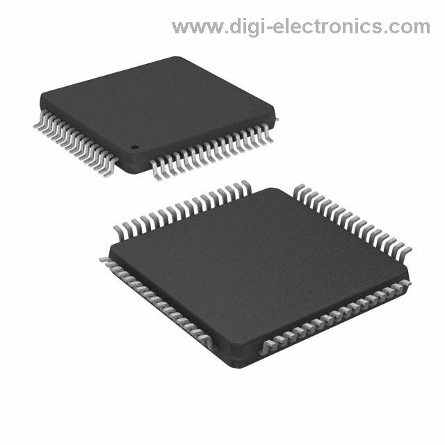
Thermal integrity and package design play a supporting but crucial role. The 64-pin TQFP (10x10 mm) package harmonizes signal density and thermal dissipation, facilitating high-density mounting without excessive board real-estate consumption. Soldering reliability and coplanarity yield a stable foundation for industrial longevity, while the pinout supports systematic routing of high-frequency signals to minimize cross-talk.
The cohesive synergy of computational performance, security hardening, peripheral breadth, and low-power aptitude embodies a scalable solution for engineers. This device’s architecture, when paired with judicious firmware design, allows for modular upgrades in both feature expansion and field updates. The platform’s flexibility fosters a forward-compatible product roadmap, facilitating the seamless integration of emerging protocols or sensor interfaces as application demands evolve.
Direct experience in integrating the EFM32WG942F256-B-QFP64 into multi-domain control units reflects the unforeseen benefits of its layered feature set. Tightly coupling signal acquisition with processing, while leveraging autonomous peripherals, yields predictable workloads and reduces MCU wake cycles. This not only improves lifecycle robustness but also simplifies electromagnetic compliance testing through streamlined signal paths.
In composite, the EFM32WG942F256-B-QFP64 demonstrates a deliberate balance between performance and integration. It stands as a strategic building block for high-reliability, future-proof embedded applications, rewarding architecture-level foresight with system-wide efficiency gains.
Key features and specifications of EFM32WG942F256-B-QFP64
The EFM32WG942F256-B-QFP64 embodies a balanced integration of computational performance, memory flexibility, and peripheral diversity, forming a robust foundation for modern embedded system design. Anchored by a 32-bit ARM Cortex-M4F processor core, it delivers processing speeds up to 48 MHz with hardware-based floating-point support. This FPU capability directly benefits real-time control loops, sensor fusion algorithms, audio analysis, and signal conditioning in scenarios where precision and deterministic latency are non-negotiable. Floating-point instructions execute efficiently, removing the code burden and cycle penalties typical of software emulation, ultimately streamlining firmware development and enabling advanced digital signal processing workloads in constrained environments.
With 256 KB of flash memory paired with ample RAM, the device supports modular firmware architectures. Memory mapping and flash organization favor secure bootloaders, field-upgradeable middleware, and complex application stacks, enabling remote update strategies and layered system protection. Memory bandwidth and latency remain optimized for both code execution and data buffering, which is especially critical in multi-threaded, RTOS-based applications that demand deterministic access times.
The packaging in a 64-pin TQFP notably increases the breadth of I/O, catering to designs requiring extensive peripheral interconnection and scalable interface options. The microcontroller provides a differentiated set of peripherals—including high-resolution timers, multi-channel ADCs/SARs, and precision DACs—targeting real-world data acquisition and closed-loop actuation. Communication modules (UART, SPI, I2C) operate concurrently, supporting fault-free node-to-node messaging in distributed control topologies like industrial automation or home energy management. These resources ensure engineering flexibility, reducing the need for costly external interfaces or custom glue logic.
Advanced power management features—such as multiple voltage scaling modes, fast wake-up, and intelligent clock gating—address the stringent demands of ultra-low-power applications. Integration with power domains and brown-out detectors mitigates system instability and data retention issues during transient supply conditions. This innate efficiency widens the scope from battery-powered consumer wearables to mission-critical field instrumentation, where both uptime and reliability are paramount.
In practice, realizing the full performance-per-watt benefit relies on meticulous peripheral initialization sequences, calibrated ADC/DAC references, and leveraging DMA for offloading repetitive transfers. Tuning system clock trees and prioritizing interrupt structures further elevates deterministic behavior. Design experience confirms that leveraging on-chip debug and trace modules during firmware development significantly shortens iteration cycles, offering granular insight into timing behavior and resource utilization.
Critically, the microcontroller’s architectural consistency, peripheral assignment, and low-level firmware interface foster rapid platform scaling—a key asset when designing product variants sharing a common hardware backbone. By aligning processing capability, interfacing bandwidth, and power efficiency, the EFM32WG942F256-B-QFP64 stands as an optimal choice for applications requiring both computational intensity and embedded reliability. Integration depth and peripheral interplay dictate a disciplined hardware-software co-design approach, ultimately reducing design risk and accelerating time-to-market for innovative embedded solutions.
Security and firmware considerations for EFM32WG942F256-B-QFP64
Robust security management is central to the deployment of high-value embedded systems, particularly when leveraging the EFM32WG942F256-B-QFP64 microcontroller. At its core, this device integrates advanced access partitioning through ARM TrustZone, tightly coupled with secure debug access mechanisms. Within such an architecture, internal permissions—specifically those governed by Debug Access Permission (DAP) bits like DBGLOCK and NIDLOCK—regulate interface availability and restrict unauthorized debug operations. This partitioning ensures that sensitive application code and debug features are physically and logically isolated, mitigating vector-based attacks at both run-time and development stages.
Firmware plays a dual role in this landscape: not only does it deliver feature sets, but it anchors the security posture by mapping lower-level hardware settings to system behavior. Recent advisories from Silicon Labs underscore the criticality of configuring TrustZone DAP bits with precision. Setting both DBGLOCK and NIDLOCK under firmware versions below 1.2.14 or 2.2.1—and then accessing the Trace Port Interface Unit (TPIU)—triggers a hardware deadlock on the ARM Cortex-M33, producing a nonrecoverable stall unless hardware-level intervention is possible. The underlying cause relates to how previous firmware handled concurrent access conflicts between secure and non-secure resources within the debug circuitry, leaving the host processor unresponsive. This effect is isolated to use cases actively engaging the TPIU; standard application execution, where trace debug channels remain disabled, proceeds without disruption.
Risk mitigation is thus both a firmware and process-centric exercise. Immediate remediation is achieved by upgrading deployment images to firmware version 1.2.14 or later, where this defect is resolved by improved internal arbitration of debug permissions. Beyond prompt upgrade cycles, process integrity demands that development and integration teams eliminate ad hoc manipulation of DAP bits outside validated configuration frameworks, especially in multi-phase testing or in-field reprogramming environments. Automated validation of security settings as part of CI/CD pipelines, paired with periodic firmware audits, sharply reduces the window for latent configuration drift that could expose critical infrastructure to stall conditions or unauthorized access.
Recovery methodologies are an essential contingency in these highly regulated deployments. The EFM32WG942F256-B-QFP64 maintains a level of resilience by providing erase-based device recovery flows. When debug locks induce nonresponsive states, enabling hardware erase allows for restoration of factory-initial conditions, reinstating debug access and full device control. However, operational best practices recommend restricting erase functions only to trusted environments, as they represent a potential attack vector if not properly controlled within supply chain and post-deployment scenarios.
The nuanced interplay between security configuration and firmware evolution illustrates the importance of continuous alignment between hardware design, firmware development, and operational processes. Proactive lifecycle management—characterized by alert tracking, rapid firmware adoption, and disciplined access control—significantly fortifies system resilience. Ultimately, the evolving threat landscape and the architectural sophistication of MCUs like the EFM32WG942F256-B-QFP64 demand systematic, awareness-driven engineering practices to maintain both functional and security integrity in deployed applications.
Application scenarios and deployment for EFM32WG942F256-B-QFP64
EFM32WG942F256-B-QFP64’s architecture centers on the ARM Cortex-M4F core, providing an optimized foundation for high-efficiency numeric processing and deterministic real-time response. The inclusion of hardware floating-point support is critical for computationally intensive tasks such as sensor fusion algorithms, advanced motor control, and complex signal conditioning. With 256 KB of flash memory, the device accommodates sophisticated firmware architectures, allowing for modular design strategies, dual-boot schemes, and dynamic feature upgrades in the field. These capabilities directly address the requirements of modern embedded systems, where adaptability and future-proofing translate into operational longevity and the ability to deliver differentiated value over time.
The comprehensive peripheral set—spanning multiple UARTs, SPIs, I²Cs, timers, ADCs, and DACs—enables direct interfacing with an array of industrial and consumer components. For instance, in high-precision measurement instruments, leveraging the device’s multi-channel ADCs, fast interrupt response, and DMA engine streamlines the path from analog input to secure digital processing, reducing latency and error. Application development benefits from pinouts supporting both high-density and fine-pitch layouts, simplifying PCB routing in space-constrained designs typical of portable test equipment, medical devices, and battery-operated sensor arrays. The QFP64 package further accelerates prototyping and field repair due to its manageable soldering profile and accessibility with mainstream PCB manufacturing processes.
Security and system integrity demand dedicated attention in deployment scenarios. The part’s native support for debug lock and code protection forms a defense against firmware extraction and malicious tampering, particularly relevant in distributed IoT nodes and industrial controllers exposed to untrusted environments. Effective use of these features requires rigorous review of the programming and debug interface configurations during both pre-production and mass deployment phases. For use cases anticipating physical access risks, implementation of debug lock protocols from initial batch programming minimizes vulnerability windows, while firmware aging policies—such as controlled update rollouts and hash-verified bootloaders—further mitigate long-term attack surface.
Field experience demonstrates that careful orchestration of peripheral activation and power modes realizes substantial energy savings, a decisive factor in edge devices with stringent battery budgets. This is accentuated by the chip’s low-power operational states and tailorable clock gating, which, when coupled with event-driven wakeup logic, sustain continuous sensor monitoring without compromising autonomy. In practical implementation of industrial automation, configuring DMA-assisted data capture and direct peripheral-to-memory channels is essential for minimizing processor load and preventing timing bottlenecks under high input rate scenarios.
Strategic adoption of the EFM32WG942F256-B-QFP64 enables deployment across a spectrum of applications, from secure data acquisition nodes in critical infrastructure to dynamic actuator control in robotics and self-adaptive consumer electronics. The platform’s versatility stems not just from its technical attributes but from a system-level approach that balances performance, security, and ease of integration—fundamental enablers when scaling from prototype validation to mass production and lifecycle management.
Potential equivalent/replacement models for EFM32WG942F256-B-QFP64
Identifying suitable alternatives for the EFM32WG942F256-B-QFP64 requires a comprehensive assessment of internal architecture, peripheral integration, and cross-compatibility within deployment ecosystems. In the context of Silicon Labs’ portfolio, the search for equivalence often narrows to other EFM32 Gecko series devices, specifically those retaining ARM Cortex-M4 or M3 cores and offering similar memory footprints—namely, flash sizes around 256KB and RAM capacities of 32KB or higher. Immediate candidates include the EFM32GG and EFM32LG lines, which yield matching performance figures and peripheral sets.
Equivalence in core performance encompasses not only processor speed but also floating point and DSP instruction support, critical for designs leveraging signal processing or complex arithmetic operations. Power efficiency parameters, such as active and standby current draw, play a pivotal role in applications where battery longevity or heat dissipation is tightly controlled. Memory allocation must align precisely to enable seamless firmware migration; microcontrollers with comparable flash sectors and SRAM organization reduce risk of fragmentation or incompatibility during code transfer and optimization.
Peripheral mix forms another crucial layer: engineers often prioritize pin-compatible devices, preserving interfaces like USB, timers, ADCs, communication buses (UART, I2C, SPI), and touch sensor support. Silicon Labs platforms typically provide consistent peripheral architecture, but subtle differences in feature set or performance banding can surface. For example, a replacement device may support additional high-speed timers or advanced analog capabilities, presenting opportunities to future-proof system requirements without disrupting PCB layouts.
Firmware compatibility warrants specialized focus, especially as embedded projects mature and accrue codebase dependencies. Ensuring substitute MCUs offer identical or superset library support—whether within the Gecko SDK or third-party RTOS environments—streamlines migration and minimizes integration overhead. Debug architectures, including SWD/JTAG availability and monitor mode behavior, should be closely matched to maintain workflow continuity across development, testing, and in-field diagnostics.
Security integration represents an advanced layer influencing model selection, particularly where TrustZone or cryptographic acceleration is necessary. Devices in the same family may differ substantially in available protection features, such as secure boot, hardware key storage, or root-of-trust formation. Evaluating cryptographic hardware blocks, ROM integrity mechanisms, and trusted execution boundaries is essential before committing to an alternative to avoid undermining application security or regulatory compliance.
Practical migration experiences highlight that even within ostensibly equivalent device lines, subtle discrepancies in errata, silicon revisions, or electrical characteristics (e.g., ESD tolerance, I/O voltage domains) can impact production stability and manufacturing yields. Proactive engagement with application notes, migration guides, and detailed electrical tables accelerates risk mitigation, enabling tighter lifecycle management.
A well-structured approach to replacement model selection, prioritized by system-level constraints and forward-looking platform scalability, consistently produces robust engineering outcomes. Carefully layered evaluation—moving from the nuances of core silicon to system integration and code portability—leads to optimal device choice, and reveals that close attention to non-obvious migration costs frequently underpins successful product evolution.
Conclusion
The EFM32WG942F256-B-QFP64 microcontroller delivers a precise balance between computational throughput, diverse peripheral support, and robust embedded security, positioning it as a strong contender in performance-critical embedded applications. At its core, the ARM Cortex-M4 processor enables deterministic real-time processing, efficiently managing both intensive algorithmic workloads and low-latency tasks. Its 256 KB flash and extensive SRAM allocation are calibrated for firmware-rich designs, accommodating dynamic updates, complex RTOS deployments, and middleware stacks without constraining application growth. Flexible GPIO mapping, advanced timer resources, and a suite of analog-digital converters streamline integration in sensor networks, signal conditioning modules, and motor control applications, where deterministic timing and high-speed signal acquisition are paramount.
Integration of security primitives, including AES hardware acceleration and advanced access control, fortifies system resilience against common threat vectors. This hardware-backed security foundation allows direct implementation of end-to-end encryption, secure boot processes, and authenticated firmware upgrades with minimal overhead, a distinguishing factor in safety-critical and connected environments. Vendor-backed lifecycle support ensures that both software maintenance and hardware roadmap alignment remain stable, reducing long-term design risk in sectors like industrial automation, medical instrumentation, and energy management.
In the context of procurement and design-in activities, critical assessment of the microcontroller’s longevity, published errata, and firmware ecosystem helps mitigate obsolescence and compatibility concerns. Teams integrating this MCU have leveraged its low-power modes to extend battery life in remote deployments without sacrificing wakeup latency. Strong documentation and an active community enable rapid prototyping cycles, with proven migration paths from evaluation modules to final product hardware.
A key insight emerges in the intersection of rich peripheral sets, aggressive power management, and flexible security integration: effective project outcomes hinge on leveraging these capabilities cohesively rather than in isolation. Designs that maximize modularity at both the software and hardware level, taking full advantage of the EFM32WG942F256-B-QFP64's broad feature set, demonstrate accelerated time-to-market and lower total system cost in demanding deployment scenarios. This microcontroller’s architecture and ecosystem collectively enable tightly coupled, resilient embedded systems where scalability and future-proofing are essential.