 >
>


Product Overview: ATF22V10C-15SI Programmable Logic Device (PLD) from Microchip Technology
The ATF22V10C-15SI represents a refined solution within the Electrically Erasable Programmable Logic Device (PLD) portfolio. Engineered on advanced CMOS flash technology, this device prioritizes high reliability and operational efficiency across demanding environments. The integration of ten flexible macrocells empowers designers with ample logic configurability, supporting complex combinational and sequential functions without peripheral complexity. Each macrocell is architected to enable tailored Boolean logic realization, enhancing circuit density while reducing layout real estate—a critical factor in both compact new systems and constrained legacy hardware.
Deployment in the 24-SOIC package drives compatibility across surface-mount workflows and eases the migration or expansion of existing products. The flash-based programmability approach yields noteworthy endurance, drastically reducing the risk of data loss and affording repeated reconfiguration without hardware depletion. Embedded efficient power management stems from optimized CMOS construction, supporting both static and dynamic applications where heat dissipation and long-term stability are paramount. Typical retention of programmed logic exceeds standard EEPROM-based alternatives, sustaining field longevity and robustness in scenarios such as industrial automation, avionics subsystems, and sensitive military infrastructure.
In typical implementation cycles, the PLD’s rapid erase-and-write cycles accelerate iterative design processes, enabling short prototyping loops and smooth late-stage adjustments during integration. For field-deployed hardware, the inherent re-programmability facilitates firmware updates and logic patching, often mitigating costly recall scenarios. The ability to program and reprogram with minimal downtime is leveraged in maintenance protocols for mission-critical deployments, where system reliability and upgradability directly impact operational continuity.
Observing the foundational mechanics, the ATF22V10C-15SI’s logic mapping is notably deterministic, supporting predictable system behavior—a facet leveraged in safety-oriented architectures. Experienced practitioners exploit the low quiescent current and high-speed reaction for integrating real-time controllers, digital interfacing modules, and signal conditioning circuits. The architecture’s inherent flexibility also lets engineers optimize for pin utilization, clock domain management, and precise timing closure, accommodating stringent electrical constraints and minimizing interference across interconnected modules.
An underlying insight emerges regarding lifecycle management: the PLD’s programmable nature extends hardware useful life, as designers can refresh and adapt logic far beyond initial deployment, responding to evolving requirements without incremental board redesign. The macrocell design, when judiciously harnessed, can serve as a bridge technology, facilitating migration from fixed-logic ICs to reconfigurable platforms—a pragmatic strategy for maintaining competitive agility in rapidly shifting markets. Operational experience underscores the value of the ATF22V10C-15SI as a scalable, resilient backbone for systems where functional evolution, reliability, and swift time-to-market coalesce into tangible engineering advantage.
Core Features of ATF22V10C-15SI
The ATF22V10C-15SI programmable logic device defines a robust solution for high-speed and power-efficient design workflows. Its electrically erasable structure forms the foundation for dynamic reconfiguration and agile prototyping, enabling streamlined iteration cycles in hardware development. When new logic requirements arise, firmware upgrades are implemented in situ without physical device swap, minimizing downtime and facilitating adaptable product life cycles. This architecture suits environments where hardware requirements are subject to frequent changes, and is particularly useful for proof-of-concept and low-volume production runs.
A key performance attribute is the minimal pin-to-pin delay—down to 5ns. This low propagation latency supports demanding timing budgets in synchronous systems, such as signal processing engines and fast bus interfaces. It enables reliable integration into high-frequency designs without violating setup and hold constraints, and ensures predictable timing for critical control paths. In practice, timing closure in dense designs often hinges on such device-level speed, with the ATF22V10C-15SI consistently meeting requirements across varying load conditions and board topologies.
Power management integrates seamlessly via pin-selectable standby mode, curtailing quiescent consumption to approximately 10μA. This mechanism supports deployment in battery-powered nodes, portable instrumentation, and other resource-constrained applications. The standby transition is hardware-driven, allowing context-sensitive sleep strategies that extend operating times between charge cycles or reduce heat generation in compact enclosures. Real-world deployment confirms that such features contribute to certification for stringent power budgets, particularly in markets emphasizing energy efficiency.
Underlying data retention leverages mature CMOS fabrication, with guaranteed integrity over extended periods—up to two decades—and resilience against frequent reprogramming. This nonvolatile storage is foundational for applications requiring configuration stability, like remote sensor arrays or system boot logic. The erase/write cycle count of 100 enables moderate refinement during installation and calibration phases without risk of premature device wear, which can be critical when fine-tuning logic in the field or maintaining legacy equipment.
Robustness is further advanced through ESD protection meeting a 2,000V threshold and latch-up immunity rated for surges up to 200mA. These safeguards mitigate risks posed by uncontrolled transients, ensuring device survival through routine fabrication, assembly, and daily operation. Field conditions—such as high static environments or unpredictable grounding—are accommodated, resulting in high reliability metrics and reducing the need for external protective measures.
Seamless compatibility with established industry-standard toolchains eliminates unnecessary learning curves or proprietary lock-in. This ecosystem integration fosters rapid assimilation into diverse workflows, from schematic capture to device programming, and supports best practices in verification and validation. Practical use confirms that design files, simulation frameworks, and utility scripts interoperate without modification, facilitating project scalability and enhancing team productivity.
The device is available in green packaging that complies with stringent environmental regulations like RoHS. This makes it suitable for deployment in products targeting regulated markets, including healthcare and automotive sectors, where compliance is not optional. The availability of such options further streamlines sourcing and avoids late design changes related to environmental audits.
Operational flexibility spans commercial, industrial, and military temperature grades, guaranteeing function under wide-ranging thermal stresses. Designs destined for mobile, outdoor, or mission-critical platforms benefit from assured operation without custom device selection, reducing validation cycles. This characteristic enables cross-sector standardization, consolidating inventory and support strategies.
Backward compatibility with legacy Atmel devices—ATF22V10B(Q) and AT22V10(L)—is integral for migration and long-term sustainment. Direct pin-level and functional equivalence ensures plug-and-play upgrades, simplifying maintenance and promoting obsolescence mitigation in complex installations.
Integrating the ATF22V10C-15SI into a design pipeline leverages a synergy of speed, reliability, programmability, and compatibility, contributing not only to project success but also to lifecycle efficiency. The holistic combination of features removes numerous constraints often encountered in programmable logic design, reaffirming the device’s relevance for forward-thinking engineering teams poised for agile innovation.
Architectural and Functional Characteristics of ATF22V10C-15SI
The ATF22V10C-15SI embodies a flexible architecture derived from Flash-based programmable logic. At the lowest level, it integrates EEPROM cells for each macrocell, enabling electrically erasable configuration. This inherently supports repeated and non-destructive logic updates. Such attributes accelerate iterative hardware validation cycles and enable mid-life system reconfiguration without the physical replacement of components.
Core to its operation are configurable sum-of-products arrays, which implement complex combinatorial and sequential circuits. The device offers support for both registered and combinatorial outputs, catering to a wide range of state machine and glue logic applications. The embedded latch mechanism stabilizes input lines, preserving established logic levels across asynchronous events and voltage transients. This function is especially valuable in high-noise or multi-voltage environments, where transient inputs commonly jeopardize deterministic operation.
System reliability is further enhanced by the distribution of robust pin-keeper circuits on each input and I/O pin. Unlike static pull-up resistors, the ATF22V10C-15SI relies on passive CMOS structures that momentarily ‘remember’ the most recent state using weak feedback. This preserves signal integrity without incurring static current draw—key for minimizing both active and standby power dissipation. As a result, predictable logic retention is achieved, extending application suitability to battery-sensitive and thermally constrained systems.
In terms of application, the architectural emphasis on electrically reprogrammable logic enables practical field updates and feature enhancements after product deployment—a capability often requested in configurable industrial controllers and consumer appliance boards. During prototyping, engineers benefit from cycle-accurate timing and minimal propagation delay, features that facilitate seamless migration from simulation to physical implementation. Furthermore, the integrated pin-keeper circuits directly counter floating input challenges encountered during board bring-up and in-circuit debugging, reducing time spent diagnosing erratic startup or margining errors.
A critical observation regarding ATF22V10C-15SI adoption is its ability to harmonize the persistence of user-defined logic with low leakage currents and minimal board footprint. Because of this balance, it effectively bridges the gap between inflexible fixed-function gate arrays and power-hungry programmable devices, positioning itself as a compelling choice in both legacy system maintenance and forward-looking rapid prototyping contexts. Such attributes reinforce its reputation as a reliable, efficient solution for designers prioritizing both logic versatility and operational stability.
Pin Configuration and Packaging Options for ATF22V10C-15SI
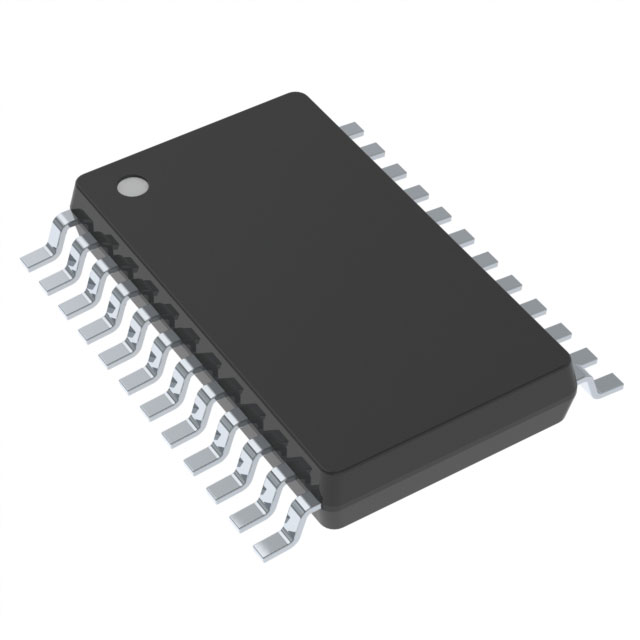
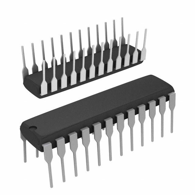
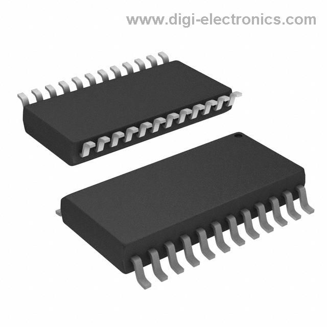
Pin configuration and packaging for the ATF22V10C-15SI directly affect design adaptability, enabling streamlined integration into diverse hardware platforms. At the silicon-interfacing level, this device’s standard 24-lead pinout ensures compatibility across the industry’s common PLD sockets, reducing long-term migration or replacement concerns. System architects capitalize on the broad availability of packages—24-SOIC for automated SMT assembly, 24-DIP for traditional through-hole mounting, 24-TSSOP where board space is at a premium, and both PLCC and LCC variants for robust socketed environments or high-reliability applications—allowing them to align component selection with both existing infrastructure and manufacturing constraints. JEDEC-compliant outlines further ensure mechanical interchangeability, simplifying logistics and supply chain management.
Strategically mapped I/O positions support predictable routing and optimal signal trace layouts, which engineers leverage for minimizing signal skew and crosstalk. The uniformity across packages streamlines prototyping and field revisions; migrating between form factors usually only requires footprint adjustments rather than comprehensive schematic redesigns. The PD (power-down) pin exemplifies the subtle optimizations available—controlled directly via hardware, it enables rapid transition to low-power states, facilitating aggressive power domains and extending operational sustainability in battery-sensitive installations. This hardware-based energy strategy enables dynamic context-aware power gating within constrained embedded systems, an often-overlooked lever for reducing overall BOM power profile.
Critical practical nuances emerge with PLCC variants, where board-level flexibility meets electrical performance. Unused pins—typically associated with programming or test features—can be optionally tied to ground or left disconnected. For speed grades other than "-5", floating pins impart layout convenience but may, under certain conditions, result in marginal timing or EMI improvements if grounded. Savvy designers exploit this by customizing unused connections in performance-critical regions or in applications facing significant electromagnetic interference, extracting non-obvious gains from meticulous package utilization. This granular approach to pin management creates subtle avenues for incremental reliability or compliance tuning in cost-sensitive mass production.
Ultimately, the ATF22V10C-15SI’s flexible packaging and pin configuration ecosystem anticipates the iterative realities of modern board engineering. Its footprint is not merely an accommodation to legacy sockets, but a platform for strategic differentiation—supporting rapid design pivots, mixed-technology assemblies, and application-specific optimizations with minimal engineering overhead. This layered versatility equips system developers to address integration, manufacturability, and field longevity, positioning the device as a building block for scalable, robust digital logic deployment.
Electrical and Timing Specifications of ATF22V10C-15SI
Electrical and timing specifications form the foundation for robust integration in programmable logic devices such as the ATF22V10C-15SI. The operational voltage range, centered at 5V with a tolerance of ±10% for militarized or industrial deployments and ±5% for commercial circuits, establishes a clear envelope for safe and reliable device behavior amid possible supply fluctuations. Respecting absolute maximum ratings—never exposing inputs to voltages below -0.6V or outputs above Vcc+0.75V DC—prevents latch-up events and long-term device degradation, mandating care in board-level interfacing, especially during transient switching or power cycling.
The definition of input AC driving levels at 0V and 3V, with timing parameters measured at a standard reference of 1.5V, ensures repeatable propagation delay and setup/hold time characteristics. This uniformity is essential in synchronous digital systems, where any ambiguity in edge detection cascades into unpredictable timing mismatches. The typical input and output pin capacitance, precisely specified at 1MHz and a controlled temperature of 25°C, quantifies load effects on signal rise and fall times. This characterization not only guides trace impedance planning but also enhances overall noise immunity, particularly in dense PCB layouts where capacitive coupling is a frequent concern.
In power-up scenarios, the integrated reset mechanism of the ATF22V10C-15SI guarantees deterministic initialization of all registers. For state machine designs, this eliminates uncertainty during startup and simplifies hardware-driven fault recovery routines. The reliability engineered into the reset circuitry also mitigates the risk of inadvertent metastable states, often a subtle source of functional instability that surfaces during temperature or voltage excursions.
Preloading support stands out as a strategic feature for testability and rapid deployment. It enables designer-directed presetting of internal register values before clock assertion, streamlining validation flows and facilitating immediate system readiness. This capability expedites boundary scan operations and reduces debug iteration times, a distinct advantage in production environments where reducing time to functional proof translates directly into throughput gains.
Layering these electrical and timing fundamentals together yields a device architecture that balances raw performance with system-level predictability. The nuanced calibration between operational voltage, interface thresholds, pin capacitance, and reset behaviours directly influences integration outcomes in diverse scenarios—from high-reliability industrial controls to agile commercial hardware. Mastery of these parameters allows for sophisticated circuit design choices, such as deliberate overdrive of certain logic inputs for noise resilience, or leveraging preload for dynamic configuration shifts during runtime.
Deep experience shows the importance of validating these specifications under just-above-threshold and just-below-threshold limits, confirming in practice how process variance affects propagation delay and initialization cycles. Iterative experiments indicate that conservative margin design, though sometimes counterintuitive in cost-targeted builds, reliably avoids edge-case failures traceable to overlooked electrical nuances or timing aberrations. The engineering discipline instilled by such thorough assessments becomes a silent force ensuring the ATF22V10C-15SI's operational consistency in the field.
Ultimately, these tightly interlinked specifications not only define device boundaries but also empower signal designers to architect resilient digital systems where timing, reset, and predictable state control converge—unlocking both flexibility and reliability in programmable logic deployments.
Power Management Features in ATF22V10C-15SI
Efficient power management within programmable logic devices is essential for optimizing resource allocation and sustaining reliable operation in diverse system environments. At the heart of the ATF22V10C-15SI’s power architecture lies its pin-controlled power-down mode, which leverages the PD pin to dynamically mitigate supply current. Activation immediately places the device into a latched state, dropping currents below 100mA while preserving all registered and combinatorial outputs. This approach safeguards signal fidelity, preventing data corruption upon return to normal operation.
The underlying mechanism is engineered through coordinated latching of internal state, with logic and output data securely retained during power-down. This guarantees that outputs resume precisely as intended with no loss or glitch, an essential property for mission-critical applications or complex embedded systems that depend on deterministic behavior following low-power cycles. Such design choices enable robust state retention, making the device suited to power-sensitive implementations, including portable instrumentation and battery-operated controllers.
An additional layer of optimization is delivered via integrated pin-keeper circuitry, working in tandem with the power-down feature. Unlike basic tri-state outputs, these circuits actively stabilize IO pins against unintended floating or leakage-induced toggling. Current consumption in standby modes is minimized, supporting stringent power budgets without risking undetected logic transitions or system noise propagation. This subtle enhancement is particularly impactful in dense logic arrays where pins may remain unassigned or inactive for extended durations.
Programming control over the PD pin is managed with fine granularity through JEDEC-standard logic files and fuse bits. Design teams can embed selective power-down logic directly within programming flows, adapting device behavior to the functional contours of the final application. This integration avoids the overhead of post-fabrication modifications, streamlining both prototyping and volume manufacturing. Practical deployment often benefits from pre-qualifying PD activation thresholds and timings under representative load conditions, yielding empirically tuned power profiles essential for high-reliability field use.
Layered together, these features reveal an architecture tailored not just for basic low-power operation but also for nuanced application adaptability and long-term reliability. The ATF22V10C-15SI exemplifies how embedded power management, empowered by programmable control and advanced pin handling, can deliver scalable solutions responsive to evolving system requirements. In scenarios demanding both minimal idle draw and instant output retention—such as remote data acquisition, safety controls, or distributed sensor hubs—the device provides an optimum platform for balancing energy constraints with performance guarantees.
Security and User Programmability in ATF22V10C-15SI
Security and user programmability in the ATF22V10C-15SI is underpinned by architectural choices designed to align with stringent industry requirements for asset protection and lifecycle management. At the heart of this approach lies the 64-bit Electronic Signature Word, an embedded programmable region that accommodates user-defined metadata—serial numbers, manufacturing codes, revision indices, or custom cryptographic tokens. Its accessibility remains unaffected by device security status, facilitating traceability and post-deployment auditing without compromising protected design logic. This flexible metadata channel strengthens system identification routines and supports fleet-level asset management within distributed deployments.
The device incorporates a hardware-level security fuse, functioning as a non-reversible lock that activates persistent memory protection. Upon blowing this fuse, access paths for verification and preload operations are permanently disabled. In practice, this mechanism secures the fuse array against unauthorized readback, thwarting iterative analysis and pattern extraction attempts inherent to reverse engineering methodologies. The one-way fuse state introduces an operational requirement: the security step should only be invoked after all programming and validation cycles have been completed. Experience indicates that integrating this action as a final sign-off in the workflow yields maximum protection while preserving development flexibility. Maintaining precise control within process automation tools—ensuring fuse activation is tightly synchronized with configuration releases—eliminates risk of premature lockdowns that could impede legitimate device reprogramming.
System integrators benefit from the device’s compatibility with industry-standard PLD programmers, which reduces learning curves and permits direct adoption into established assembly lines. The uniform interfacing protocols facilitate seamless tooling transitions and enable parallel multi-unit programming, critical for high-throughput environments. The absence of proprietary or complex programmer requirements supports modular development, allowing teams to synchronize hardware configuration and software deployment activities.
A distinctive strength of the ATF22V10C-15SI design is its reconciliation of robust security with operational flexibility. By partitioning security and user data storage capabilities, the device unlocks differentiated application scenarios—secure feature activation, field-based update logging, lifecycle tracking—without exposing core logic patterns to unauthorized analysis. The layered protection model offers nuanced control over device states, catering to both security-sensitive deployments and traceability-driven solutions. This synthesis of hardware-level policy enforcement with user-accessible metadata storage forms a foundation for both resilient IP protection and scalable system oversight.
Engineering Integration: Application Scenarios and Compliance for ATF22V10C-15SI
Engineering integration of the ATF22V10C-15SI hinges on its robust architecture and exceptional flexibility. This GAL (Generic Array Logic) device operates reliably at 5.0V, catering to diverse operational demands, including glue logic replacement, DMA controller logic, sequencer implementations in FSMs, and certain graphical data path operations. Its logic cell structure offers programmable AND-OR plane interconnects, facilitating the synthesis of custom logic functions or rapid adaptation of legacy designs as requirements evolve.
Deep integration is supported through predictable timing characteristics and deterministic propagation delays, affording precise control within high-speed digital pipelines. This feature is especially relevant in timing-critical applications, such as interfacing memory or peripheral devices with DMA engines or implementing control planes in complex state machines. Designers can leverage low standby currents and fast switching speeds, optimizing power-performance tradeoffs for both mission-critical and energy-sensitive deployments.
The device’s PCI compliance ensures straightforward incorporation into shared bus architectures, eliminating ambiguity in electrical signaling and timing, which is crucial for both forward-compatible and backward-compatible board designs. The wide ambient temperature range and support for multiple package footprints—ranging from DIP for prototyping to PLCC for production—expand deployment flexibility. Ruggedized variants tolerate significant mechanical and thermal stress, enabling installation in harsh field conditions, including outdoor control panels and military-grade enclosures where continuous reliability is essential.
In practical terms, integrating the ATF22V10C-15SI often involves rapid prototyping using in-circuit reprogrammability and secure lock-bit protection for IP-sensitive applications. Adaptation of the programmable fuse array streamlines late-stage design changes, reducing overall project turnaround without sacrificing reliability. Field observations reflect resilience in maintaining signal integrity and logical coherency despite EMC noise or voltage fluctuations, facilitating long-term support for legacy equipment, as well as integration into contemporary mixed-voltage platforms via robust level-shifting schemes.
One distinctive advantage emerges from the convergence of high pin compatibility and flexible programming: teams can incrementally upgrade deployed products, gradually phasing in enhanced logic capabilities and improved signal management without wholesale redesign. This modularity catalyzes innovation while protecting prior investments, supporting iterative engineering cycles common in industrial automation and aerospace control systems. The ATF22V10C-15SI’s footprint in both legacy maintenance and forward-looking systems underscores a unique equilibrium between stability and adaptability, central to sustainable hardware platform evolution.
Potential Equivalent/Replacement Models for ATF22V10C-15SI
Selection of ATF22V10C-15SI alternatives within the programmable logic device (PLD) category demands a careful mapping of the selected model’s functional profile against the performance and compatibility constraints of the application environment. The Atmel ATF22V10B(Q) is characterized by its backward compatibility, retaining the pinout and programming requirements of the original part. The device’s functional equivalence and consistent switching characteristics simplify drop-in replacement scenarios, minimizing the risk of timing violations or logic resource mismatch during board upgrades. This positions it as an optimal choice when continuity of legacy designs and low migration effort are prioritized.
The Atmel AT22V10(L) model further expands the selection horizon, maintaining alignment with core device architecture but subtly differing in process enhancements and operational parameters. Careful attention to voltage thresholds, propagation delay, and output drive specifications is essential when finalizing substitutions, as even minor shifts can impact critical setup/hold margins at the system level. When transitioning between these components, examination of their JEDEC programming files and cross-toolchain compatibility reduces integration friction, especially in environments utilizing legacy HDL flows or proprietary toolsets.
Engineering practice underlines the necessity of evaluating package footprints and thermal characteristics, particularly in applications subject to tightened board layouts or extended temperature requirements. Pin-compatible variants streamline PCB revisions and mitigate soldering risks, yet differences in junction temperature tolerance or quiescent power draw may dictate solution selection, especially in precision or mission-critical deployments. Moreover, given the evolving support matrices of vendor software, early validation of development suite compatibility accelerates device programming cycles and preserves test coverage integrity.
The nuanced interplay between device selection and system context suggests a multidimensional approach, balancing immediate form-function equivalence with forward-looking concerns such as supply chain continuity, obsolescence-protection, and scalability. A refined substitution strategy leverages these underlying mechanisms—standardized architectures, programmable flexibility, and ecosystem interoperability—to engineer resilient, future-proof solutions for PLD-centric assemblies.
Conclusion
The ATF22V10C-15SI stands out as a programmable logic device engineered for robust performance and adaptability within modern electronic architectures. At its core, this PLD utilizes a flexible macrocell configuration that supports both combinational and sequential logic, enabling efficient implementation of custom functions. The device’s high-speed operation and low propagation delay contribute significantly to timing-critical designs, such as real-time control systems and data communications interfaces. Advanced power management features are integrated at the silicon level, ensuring minimal static and dynamic power consumption, even in complex circuit topologies. This efficiency supports deployment in battery-sensitive and energy-conscious scenarios, from portable instrumentation to communication nodes.
Package versatility extends deployment possibilities across a range of board layouts, facilitating seamless integration into diverse hardware platforms. For design migration and legacy support, the ATF22V10C-15SI’s backward and forward compatibility mitigates risks associated with supply chain transitions and future product upgrades. Its security features enforce reliable protection against unauthorized reconfiguration, a critical factor when safeguarding intellectual property and maintaining operational integrity in connected systems.
From initial device selection to field application, the ease of programming and reconfiguration minimizes engineering overhead. Empirical data from iterative prototyping demonstrates the reliability of its configuration retention and rapid deployment across production batches. In high-mix product environments, the device simplifies logistics by reducing the need for multiple PLD variants. Notably, the comprehensive feature set encourages modular design practices, supporting scalable architectures without sacrificing signal integrity.
The intersection of architectural resilience and system-level interoperability positions the ATF22V10C-15SI as a strategic asset in electronic solution development. Integration efficiency, combined with consistent performance across temperature and voltage extremes, makes it suitable for both legacy platform renewal and cutting-edge innovations. By leveraging its adaptability, product selection and design optimization initiatives are empowered to deliver designs that remain competitive and resilient to evolving technical standards.