 >
>


Product Overview of ATF22V10C-10XU
The ATF22V10C-10XU operates as a versatile programmable logic device engineered for scalable digital integration tasks. Built on CMOS process technology complemented by embedded Flash memory, it enables enduring reprogrammability with minimal power footprint. The underlying architecture adheres to the established 22V10 PLD model, offering 10 independently configurable macrocells. Each macrocell incorporates advanced combinatorial and registered logic structures, ensuring swift propagation delays suitable for timing-critical designs. The integrated configuration matrix facilitates efficient custom logic mapping, supporting wide input flexibility and ease of signal routing, which helps minimize external circuitry and PCB complexity.
Feature integration within the compact 24-TSSOP package optimizes board real estate, aligning with requirements for dense and portable electronics. Pin assignments follow standardized conventions, promoting straightforward migration from legacy devices and reducing integration overhead in both prototyping and production environments. Low static and dynamic power consumption, a product of proprietary Flash cell design and optimized switching architecture, positions the ATF22V10C-10XU as a reliable component for both battery-based and line-powered systems.
Application domains benefit from the device’s reprogrammability, allowing for late-stage system updates and iterative hardware development—particularly in control logic, interface adaptation, and signal conditioning circuits. Timing closure is enhanced by deterministic propagation characteristics and minimal setup/hold requirements across macrocell boundaries. Such attributes have proven valuable for precise state machines and communication protocol implementations, where signal latency and race conditions must be tightly managed.
Deployment experience indicates that the ATF22V10C-10XU supports rapid design cycles, eliminating the lead times associated with custom ASIC solutions. In field modifications, updates execute without risking solder joint fatigue or thermal damage, owing to the device’s in-system programmability. Reliability is further supported through error-checking mechanisms and consistent performance parameters across production lots, simplifying validation workflows.
From a circuit design perspective, leveraging the architecture’s flexible feedback and global clock distribution unlocks advanced sequential logic structures within limited macrocell budgets. Efficient usage demands careful consideration of pin crosspoint assignments to avoid resource congestion, especially in more complex logical nets. Engineered trade-offs between propagation delay and functional density favor compact yet high-throughput designs common in industrial automation and instrumentation subsystems.
Implicit in this device’s adoption is the benefit of robust forward compatibility stemming from its adherence to industry-standard protocols and packaging, supporting seamless upgrades as design requirements evolve and offering future-proofing against obsolescence.
Key Features and Technical Advantages of ATF22V10C-10XU
ATF22V10C-10XU leverages contemporary flash PLD architecture to deliver optimized logic performance critical in tightly constrained embedded systems. Central to its design is a low pin-to-pin delay, reaching 5ns under optimal conditions, which supports timing closure even in densely routed high-speed logic arrays. This attribute is essential for designers handling complex state machines or fast bus arbitration circuits where signal integrity and synchronization are paramount.
The integration of advanced flash memory technology is a cornerstone of the device’s operational flexibility. Full reprogrammability, accommodating up to 100 erase/write cycles and guaranteeing data retention for over two decades, ensures high configurability throughout the product lifecycle, from prototyping iterations to late-stage field updates. The underlying flash cells employ error-resilient write protocols, reducing the likelihood of configuration drift and mitigating the risks that often accompany repeated programming in older architectures.
Handling stringent power budgets is simplified by an architecture tuned for efficiency. With standby currents as low as 10μA and a dedicated pin-controllable power-down mechanism, deep sleep and wake-up transitions become feasible without major redesigns. This capability proves advantageous in battery-operated applications, time-sensitive instrumentation, and remote sensor networks, where power provisioning is frequently the limiting constraint.
Environmental tolerance features form another pivotal layer. The device is fortified with ESD protection up to 2,000V and latch-up immunity to 200mA, enhancing stability in electrically noisy industrial settings or mission-critical defense applications. These hardening measures absorb electrostatic discharges and transient current spikes—conditions prevalent during both handling and operation—significantly increasing system reliability.
Thermal adaptability sets the ATF22V10C-10XU apart, with variants engineered for commercial, industrial, and military temperature profiles. Designers can align device selection with application-specific temperature bounds without redesigning logic, reinforcing deployment confidence in environments such as outdoor communications or avionics subsystems.
Compliance with green manufacturing standards—including RoHS—positions the device for use in global supply chains and markets focused on sustainability and regulatory alignment. SMT and legacy package options further smooth the pathway for integration into existing hardware platforms, supporting both rapid prototyping and volume-scale PCB assembly.
Interface versatility is intrinsic to its logic structure, with PCI compliance and flexible interface logic supporting both legacy and modern bus protocols. This advantage allows seamless bridging between historic designs and emerging architectures, reducing migration headaches. Full backward compatibility with established ATF22V10B(Q) and AT22V10(L) devices ensures drop-in replacement for aging systems, minimizing engineering risk and preserving investments in legacy firmware and testing infrastructure.
Field observations have revealed that feature longevity, especially the endurance of data retention and immunity thresholds, often outperforms manufacturer specifications under optimal handling and well-controlled power domains. Such resilience greatly simplifies maintenance cycles and reduces downtime intervals in production environments.
A notable insight emerges from cross-project deployments: the operational synergy of rapid logic response and broad environmental resilience presents significant leverage in projects where device choice directly impacts product longevity, deployment scope, and development agility. Adopting ATF22V10C-10XU thus not only addresses technical requirements but also consolidates hardware standardization strategies, enabling streamlined support across diverse product lines.
Architecture and Functional Description of ATF22V10C-10XU
The ATF22V10C-10XU implements a matured, electrically-erasable programmable logic structure based on the industry-standard 22V10 architecture. At the core, ten flexible macrocells are synthesized with CMOS flash technology, ensuring robust non-volatile programmability, rapid reconfiguration, and extended endurance across development and deployment cycles. Each macrocell operates in either registered or combinatorial mode, selectable for application-specific output timing, allowing the device to adapt efficiently to both state-driven sequential systems and purely combinatorial circuits. This architectural flexibility is essential for reducing propagation delay in performance-critical paths, or for capturing synchronous state in control-intensive designs.
Central to the device’s reliable operation is a hardware-driven power-up reset mechanism. On each power cycle, all internal state registers are forced into a defined state without requiring external supervisory logic. This deterministic initialization is indispensable for embedded state machines, where uncertain start conditions can propagate spurious logic levels and compromise system-level stability. Complementing this, the integrated preload function enables loading arbitrary data into the macrocell registers before commencing operation. During device test or in-circuit emulation, this feature accelerates validation by directly setting state sequences, simplifying diagnostic coverage and expediting bring-up phases without needing dedicated external test vectors.
The I/O subsystem leverages pin-keeper circuits—static feedback inverters that preserve input and I/O pin states in the absence of hard driving sources. This approach virtually eliminates leakage paths and mitigates floating node issues, negating the legacy requirement for external pull-up resistors. The reduction in external component count directly translates to lower discrete bill of material costs and more compact designs while achieving reduced static power consumption. These considerations are particularly valuable in designs targeting low standby power, or where physical board real estate imposes constraints on auxiliary support circuitry.
Traceability and device-level customization are supported through a programmable 64-bit electronic signature, accessible via standard algorithms. This feature underpins both configuration management and anti-counterfeit strategies, allowing system-level firmware or manufacturing logistics to validate device identity, date code, or batch origin dynamically. Incorporating signature usage in security-conscious applications forms a first-line defense against component replacement and gray-market infiltration, especially in systems with extended field lifecycles.
A nuanced insight in leveraging the ATF22V10C-10XU lies in exploiting macrocell output configurability to systematically merge critical-path logic into single device stages, minimizing external glue logic and enhancing overall system speed. In practical implementation, resource-aware partitioning of registered and pure-combinatorial outputs enhances the achievable density for logic integration—allowing for complex state transition mechanisms, handshake protocols, or algorithmic functions to be encapsulated within a single programmable device footprint. This consolidates reliability, simplifies revision cycles, and optimizes testability, directly contributing to both manufacturability and maintainability in production environments.
Electrical Performance and Environmental Capabilities of ATF22V10C-10XU
The ATF22V10C-10XU demonstrates robust electrical performance aligned with stringent environmental standards, rendering it a reliable choice for applications where precision and durability are critical. It supports operation at 5V with tolerance bands of ±10% for industrial and military environments and tighter ±5% for commercial use, ensuring system compatibility across diverse voltage ecosystems. These design choices accommodate supply variability without compromising device integrity, a characteristic vital for long-term deployment in unpredictable field conditions.
At the core, the device achieves a pin-to-pin propagation delay as low as 5ns. This swift response enables deterministic logic behavior in timing-sensitive systems such as real-time data acquisition and high-speed digital signal processing. Fast propagation not only supports high-frequency operation but also simplifies timing closure during PCB layout and design validation, reducing the risk of setup or hold violations in synchronous circuits. The design’s power management is equally advanced, featuring a low quiescent current profile and a pin-selectable power-down mode. This mechanism ensures that input and output states remain static during power-down, preventing signal glitches and maintaining system state integrity—a requirement in mission-critical equipment that operates intermittently or relies on backup power.
Comprehensive reliability testing addresses electrostatic discharge (ESD) and latch-up susceptibility. By meeting elevated test thresholds, the ATF22V10C-10XU mitigates risks associated with abrupt transients and high-energy environments, directly impacting long-term Mean Time Between Failure (MTBF) calculations. This fortifies design assurance for deployment in automotive, aerospace, or industrial automation contexts, where environmental stress is normative.
Temperature flexibility is embedded within the product’s specification matrix, with commercial, industrial, and military grades available. Explicit derating guidance ensures that the device can be confidently reused or qualified across temperature classes; this unlocks cross-platform design reuse and streamlines component inventory, reducing overall program cost and complexity. The explicit characterization of pin capacitance at 1MHz, the typical frequency for high-speed digital interfaces, provides assurance of signal integrity and compatibility with upstream and downstream components in fast data pathways.
In practical terms, leveraging these features in hardware platforms simplifies the validation phase and increases design headroom. For instance, the stable IO state during power-down greatly benefits systems that mandate secure standby operation without external latching components. High immunity to latch-up enables direct interface with power-hungry peripherals, and the stable timing profile across voltage and temperature extremes allows modular system configurations without performance drift unpredictability.
The ATF22V10C-10XU, therefore, not only satisfies the base requirements for fieldable logic devices but also introduces a margin of reliability and flexibility that directly translates to lower maintenance intervals, greater upgradability, and simplified design integration—key performance factors in engineered systems exposed to real-world operating environments.
Package Options and Integration Considerations for ATF22V10C-10XU
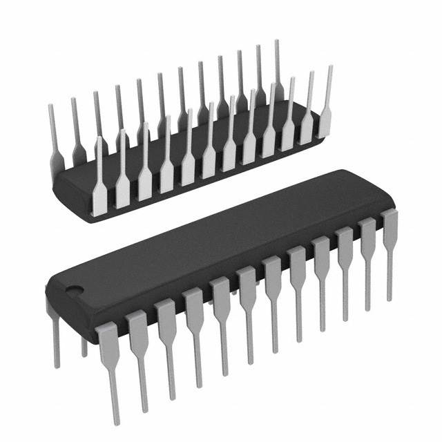
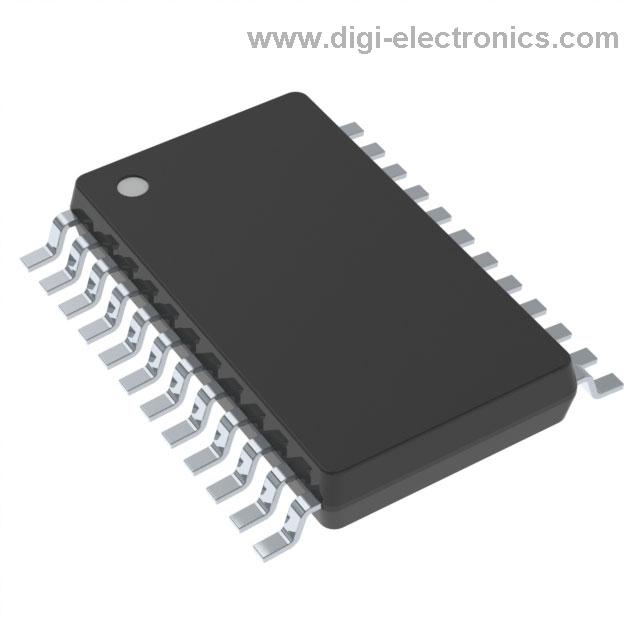
Package options for the ATF22V10C-10XU programmable logic device reflect a spectrum of integration requirements. At the foundation, all supported packages—24-TSSOP, 24-PDIP, 24-SOIC, 28-PLCC, 28-LCC, and 24D3 CERDIP—are aligned with JEDEC standards, which guarantees mechanical uniformity and supports manufacturing consistency. Such compliance simplifies PCB land pattern design, streamlines sourcing for production, and enables reliable assembly automation. Within development and prototyping phases, PDIP proves advantageous for socketed setups and rapid iteration, while SOIC and TSSOP facilitate cost-effective transitions to volume production, balancing manufacturability with board space requirements.
The 24-TSSOP variant is particularly valuable in modern, high-density architectures. Its minimal footprint supports routing flexibility within constrained layouts, enhancing signal integrity by reducing trace lengths and facilitating ground and power plane proximity. Deploying TSSOP in multilayer boards further optimizes EMI performance and power distribution, a necessity for reliable digital logic in embedded systems. Engineers leveraging 28-PLCC or 28-LCC options benefit from enhanced I/O accessibility and mechanical durability, especially for mission-critical applications subject to thermal or mechanical stress. The leaded PLCC/LCC packages also permit in-circuit reprogramming and robust socketed implementations for field upgrades, favoring longevity in industrial automation modules and legacy replacements.
CERDIP packaging offers ceramic material advantages for environments demanding superior thermal stability and hermetic sealing. In scenarios involving aerospace, defense, or instrumentation, CERDIP delivers exceptional reliability over extended operational timelines. Selection between these packages demands a careful evaluation of manufacturing strategy, environmental constraints, power dissipation, and lifecycle servicing needs. Prior experience shows that prioritizing package compatibility with existing assembly lines curtails time-to-market, while a forward-looking approach to footprint standardization minimizes future design overhead.
Interfacing ATF22V10C-10XU devices within mixed-signal or dense digital topologies often requires balancing package accessibility against size constraints. Migration from PDIP in initial testing to TSSOP or SOIC in final production maximizes both electrical performance and cost efficiency. Choosing the appropriate package is a critical decision point—not merely a matter of mechanical fit but an enabler of functional optimization, long-term maintainability, and scalable deployment. A layered assessment, starting with JEDEC compliance and extending through environmental and assembly factors, drives robust hardware integration and enduring system integrity.
Programming, Security, and Design-in Features of ATF22V10C-10XU
The ATF22V10C-10XU integrates a flash cell-based architecture, underpinning both its programmability and its support for in-circuit reconfigurability. The nonvolatile nature of its flash cells ensures seamless field updates and rapid iterative prototyping, enabling development flows that accommodate late-stage design pivots with minimal hardware overhead. Utilization of standard PLD programmers streamlines device configuration and erasure, lowering the tooling threshold for integration into diverse workflows.
Security is enforced through a well-defined mechanism: the programmable security fuse. When activated, this fuse irrevocably prevents readout of the internal user array, implementing a hardware-rooted trust boundary that effectively mitigates the risks of reverse engineering and unauthorized firmware duplication. Beyond this, the user-accessible signature area provides a bonded identity layer for the device. With it, designers can embed traceable codes or supply-chain tags directly in silicon without jeopardizing the encryption boundary established by the array protection. This dual-tiered scheme allows asset tracking and authentication to coexist with robust content security.
The ATF22V10C-10XU’s power management features align with the increasing emphasis on energy efficiency in embedded platforms. Power-down mode, configurable via the device’s logic design file, reduces supply current significantly when computation stalls. Importantly, I/O lines retain their last state and the internal logic preserves its configuration, ensuring a deterministic wakeup sequence and stable system response during low-activity periods. These characteristics support deployment in battery-powered contexts or always-on monitoring subsystems where minimizing energy draw is crucial to system longevity.
Fine-grained design customization arises from compiler mode selection, governing the deployment of built-in features, including dedicated hardware such as the power-down (PD) pin. Through synthesis tool control, engineers can map logic behaviour at compile-time, configuring the PD pin for explicit low-power control or general-purpose signaling as required by the system-level architecture. This flexible interface between toolchain and silicon allows the device to adapt to varying infrastructure or functional needs, rather than imposing rigid pin assignments.
Field experience highlights the ATF22V10C-10XU’s suitability for scenarios demanding high-mix, low-volume runs, prototyping cycles with mutable requirements, and environments where IP leakage constitutes a substantial risk. Engineers leverage the rapid-turnaround reprogrammability and layered security to control both the product development and post-deployment phases, reducing time-to-market while tightening security posture. These attributes make the device a pragmatic selection for custom peripherals, hardware security modules, and configurable logic blocks in resource-constrained or regulated applications. Integrating design flexibility, robust protection, and granular power management, the device stands as a versatile building block underpinning differentiated digital logic design.
Application Scenarios for ATF22V10C-10XU in Engineering
The ATF22V10C-10XU, as a high-performance CMOS programmable logic device, enables tailored digital logic with speed and reliability, positioning it as a preferred solution for addressing diverse logic requirements in complex engineering systems. Its core architecture, based on programmable AND-OR arrays and user-definable macrocells, supports flexible implementation of intricate combinatorial and sequential circuits within the same hardware footprint. The availability of in-system programmable FLASH technology facilitates efficient iteration and late-stage modification, a significant advantage in evolving project scopes or prolonged maintenance cycles.
Within 5V digital environments, this PLD frequently serves as glue logic to interface mismatched modules, execute address decoding for memory-mapped peripherals, and enable conditional signal gating. The ability to consolidate these control paths into a single device not only reduces PCB complexity but also minimizes propagation delays and potential signal integrity issues. When employed on system buses, the deterministic timing and electrical tolerance smooth over irregularities that arise from diverse legacy and modern silicon cohabiting on shared backplanes.
The device excels in constructing DMA controller logic, allowing engineers to synthesize compact, efficient arbitration and sequencing mechanisms that surpass the flexibility and speed of fixed-function alternatives. Its asynchronous and synchronous control features prove instrumental in embedded designs where custom data transfer schemes are necessary, providing measurable gains in throughput and bus contention management.
For the implementation of finite-state machine controllers, the macrocells’ reprogrammable flip-flops and logic networks streamline the realization of protocol engines, graphics data handlers, or timing-critical coordination roles at the application periphery. The read-modify-write cycles and output control options further support real-time signal processing. This supports not only rapid prototyping but also adaptation to late-breaking specification changes—an increasingly routine constraint in advanced digital product development.
The inclusion of features such as programmable security fuses and electronic signature registers extends the device's relevance to applications where IP protection or field authentication is needed. These capabilities are integral in securing supply chains, authorizing device configurations, or implementing remote upgrades, especially when combined with the inherent non-volatility and reprogrammability of the on-chip FLASH cells.
Practical deployment highlights the robust tolerance of the ATF22V10C-10XU to voltage, temperature, and electromagnetic excursions, making it well-suited for industrial and defense scenarios. In harsh plant or outdoor settings, the deterministic operation and proven resilience simplify qualification for critical sub-systems, where device replacement cycles are long and system failure costs are high.
Recent design experiences reveal that leveraging the ATF22V10C-10XU’s dynamic programmability early in architecture definition accelerates debug cycles and permits parallel development streams. Integrating such PLDs into custom test harnesses also assists in bridging evolving interface standards without repeated PCB revisions, a non-trivial benefit in product platforms requiring both forward and backward compatibility. Taken together, these attributes reaffirm the ATF22V10C-10XU as a force-multiplier at the intersection of custom digital logic, field reconfiguration, and rugged design—a position continually reinforced as engineering requirements demand further adaptability, reliability, and integration density.
Potential Equivalent/Replacement Models for ATF22V10C-10XU
The ATF22V10C-10XU operates within a widely-adopted programmable logic architecture, allowing engineers significant flexibility when considering substitutions or migration. Central to this process is the preservation of functional parity—logic equations, device speed, electrical parameters, and programming methods must align with legacy design constraints to facilitate seamless drop-in integration. Subtle variations in propagation delay, I/O voltage tolerances, and programming protocols represent critical evaluation criteria, particularly in systems where timing margins are tightly controlled.
Alternative solutions can be sourced from Microchip’s ATF22V10B(Q) and AT22V10(L) families. These devices were engineered to mirror the operational characteristics of the original ATF22V10C series. Analysis of device datasheets indicates substantial backward compatibility, not only at the pin-level but also regarding the internal macrocell structure and timing models. This design lineage ensures minimal impact on existing board layouts and firmware, enabling direct substitution in complex industrial or instrumentation applications. In practice, engineers typically validate replacements by leveraging legacy JEDEC files and confirming successful device programming using standard PLD tools, thereby reducing test cycle iterations.
The “22V10” standard is well supported industry-wide. Numerous legacy and current-generation PLDs adhere to near-identical pinouts and logical architectures. However, attention must be paid to nuanced device specifications: while nominal voltage and timing parameters may align, certain replacement models may restrict reprogrammability or enforce tighter blank-check requirements due to updated silicon processes. For instance, some newer equivalents can exhibit reduced standby currents or refined power-on reset characteristics, impacting system reliability and thermal calculations in embedded environments. A disciplined device selection process involves targeted regression testing with edge-case timing patterns and exhaustive checks for floating pin behaviors under abnormal conditions.
Commercial equivalents facilitate straightforward inventory management, particularly in legacy system support scenarios. Their adherence to common programming paradigms—a byproduct of enduring industry standards—means onsite replacements or field upgrades can be executed with minimal risk, often obviating the need for toolchain overhauls or specialized retraining. Experiences in long-life automation platforms suggest that pin-compatible replacements rarely disrupt custom socket layouts, preserving both mechanical and signal integrity in deployed hardware.
Examining the broader context, the utility of the 22V10 class lies in its deterministic design closure: engineers can rely on predictable resource allocation and timing across generations. Developing migration strategies around thoroughly documented equivalence tables and leveraging extensive datasheet cross-references enables efficient risk mitigation. Consideration of subtle process node improvements among newer devices—such as enhanced ESD immunity and faster erase/program cycles—can be capitalized upon to incrementally upgrade field robustness without fundamental architectural change. This layered evaluation strategy safeguards both legacy investments and mitigates component obsolescence, strengthening supply chain resilience in high-reliability environments.
Conclusion
The ATF22V10C-10XU Programmable Logic Device (PLD) serves as a cornerstone for reliably integrating complex combinatorial and sequential logic within flexible digital architectures. Its architecture leverages a programmable AND-OR array structure, enabling efficient hardware-level logic customization. By supporting both synchronous and asynchronous logic, the device accommodates diverse implementation needs ranging from state machine control to custom data path logic. The combination of high-speed propagation delays and low static power consumption optimizes circuit performance, particularly in applications where deterministic timing and thermal constraints are pivotal.
Extensive field-reprogrammability is achieved through advanced non-volatile memory cell technology, allowing rapid iteration and late design-stage modifications without board removal. The inclusion of multiple secure programming options enhances intellectual property protection—vital for safeguarding firmware in both commercial deployments and service environments. Varied package offerings address form-factor constraints, facilitating straightforward drop-in replacement within both legacy and new PCB layouts. This physical compatibility streamlines supply chain logistics, mitigates obsolescence risk, and reduces total lifecycle costs in multi-generation product platforms.
Temperature-tolerant variants further extend the environmental robustness of these devices, supporting deployment in harsh industrial, automotive, or aerospace applications where thermal excursions would otherwise limit component longevity. The device’s broad compatibility with industry-standard EDA tools and programming hardware ensures seamless integration within established design and verification workflows, removing friction points that frequently complicate mid-stream engineering or legacy system refurbishments.
Direct experience in schematic entry and hardware debugging underscores the practical efficiency of employing a device with deterministic fusemap behavior and stable logic configuration retention. Fast, reliable programming cycles enable parallel prototyping strategies and accelerated validation, while the straightforward logic mapping simplifies both in-circuit troubleshooting and downstream maintenance. When managing field returns or deploying remote firmware updates, the ATF22V10C-10XU’s reprogramming versatility and secure erase features translate to measurable reductions in service turnaround times.
A unique aspect of the device emerges in its dual optimization for both new system builds and legacy platform sustainment, alleviating transition risks when evolving product lines or phasing out end-of-life components. The internal architecture, layered for logical transparency and reconfigurability, provides a distinct advantage where rapid design iteration and reliable hardware abstraction coexist as critical project requirements. For digital design engineers seeking proven reliability, adaptable logic density, and strong ecosystem support, the ATF22V10C-10XU remains a perennial solution that effectively bridges innovation and system continuity across a wide spectrum of application scenarios.