 >
>


Product Overview: CY7C1079DV33-12BAXIT High-Speed SRAM
The CY7C1079DV33-12BAXIT occupies a distinct position in the landscape of high-speed static random-access memory, leveraging a 32-Mbit (4M × 8 structure) organized for uncompromising data access fidelity. Engineered in a 48-ball FBGA configuration, the device exploits the twin benefits of compact footprint and improved signal integrity, attributes that remain critical as board real estate becomes increasingly contested in modern system designs.
Delving into the device architecture, this SRAM features a true asynchronous core that eliminates clock dependency, enabling immediate data availability upon valid address and chip selection. This design, coupled with an industry-leading access time of 12 ns, minimizes latency in closely coupled processor-mapped memories. The asynchronous protocol supports parallel access scenarios with predictable, deterministic read/write timings—qualities essential in real-time control loops, packet buffers for network switches, and high-frame-rate imaging systems. Furthermore, fully static operation dispenses with refresh cycles, resulting in straightforward timing analysis and eliminating refresh-induced nondeterminism, thereby promoting system reliability in embedded environments.
Robust data retention is assured, thanks to low leakage FET and cell designs, which demonstrate operational stability across extended temperature ranges and supply voltages (3.3 V ±0.3 V). This characteristic enhances suitability in applications exposed to industrial temperature swings or modest power supplies, such as field-deployed communications infrastructure or robust automotive microcontrollers. FBGA packaging reinforces this robustness, delivering low inductance and tightly controlled impedance, crucial for maintaining signal integrity at high load speeds, especially where line reflections and crosstalk can become limiting factors in memory bus design.
From the perspective of system integration, the device offers simple interface logic, compatible with standard TTL inputs and unambiguous data valid signals, streamlining connectivity to FPGAs, microprocessors, or custom ASICs. Designers benefit from the lack of bus arbitration overhead and the ease of implementing multi-bank parallel memory schemes for expanded bandwidth or fault tolerance. In practical deployment, careful PCB layer stack-up planning and trace impedance matching are imperative to fully harness the speed advantages, particularly when deploying multiple SRAMs in parallel to scale throughput.
Continuing advances in parallel processing algorithms and deterministic control further reinforce the relevance of low-latency, asynchronous SRAM like the CY7C1079DV33-12BAXIT. In prototyping complex digital systems, substituting synchronous burst RAM with this device often reveals that the absence of clocking constraints translates to significant reductions in timing closure effort and a lower risk of inadvertent wait-state insertion, a valuable advantage as the sophistication of application logic grows.
In high-speed design ecosystems, the CY7C1079DV33-12BAXIT’s operational efficiency, compact size, and robust timing characteristics position it as a pivotal component when predictable memory behavior, low access time, and physical resilience are non-negotiable. Choosing this SRAM, especially when board complexity or speed demands make alternative solutions less practical, directly impacts overall system responsiveness and architectural simplicity. The nuanced trade-off between density, speed, and ease of integration must be weighed, yet for demanding real-time or bandwidth-intensive applications, this device consistently delivers optimized performance.
Key Features and Performance Highlights of CY7C1079DV33-12BAXIT
The CY7C1079DV33-12BAXIT static RAM integrates advanced feature sets across speed, power efficiency, and interface compatibility, responding to the stringent requirements of modern high-throughput system design. Its 12 ns access time is achieved by refined read path architecture leveraging optimized word-line drivers and sense amplifiers, lowering response latency for critical sections within network appliances, signal processing modules, and embedded control units. Sustained high-speed data cycles are feasible without imposing excessive burdens on surrounding logic, particularly where deterministic memory response is pivotal for real-time transaction handling or fast packet buffering.
On the power profile, the device demonstrates a finely tuned active current specification—250 mA at peak speed—enabling efficient operation under continuous load without exceeding thermal budgets in compact enclosures. The ultra-low 50 mA standby current, retained even during prolonged idle states, empowers system designers to implement aggressive sleep modes while safeguarding data integrity. Data retention down to 2.0 V supports battery-backed applications and scenarios requiring extended data persistence during power transitions or glitch events. These attributes converge to permit both intensive, mission-critical compute bursts and periods of extended system dormancy with minimized energy overhead.
The memory employs robust CMOS process fundamentals, ensuring high-noise immunity and operational stability across irregular power or signal conditions. Full TTL-compatible I/O senses and outputs are architected to facilitate seamless integration with legacy system boards and hybrid subassemblies, streamlining migration and upgrade cycles. In practice, the option for single or dual chip-enable inputs unlocks versatile bank switching or parallel memory expansion across distributed address spaces, simplifying board routing and providing deterministic control over individual memory domains. Automatic power-down intelligence when not selected actively reduces cumulative system dissipation, a crucial factor in multi-device arrays or densely packed PCBs.
The 48-ball FBGA package balances signal fidelity and mechanical resilience; its Pb-free, RoHS-compliant construction aligns with sustainability mandates. The small footprint and optimized pinout aid in high-frequency signal management, yielding superior PCB utilization and minimizing cross-talk in designs where layout complexity directly impacts system bandwidth. Deployments in industrial automation, switch fabric controllers, and custom peripheral modules benefit from the device's marriage of moderate density and rapid parallel random access, especially in scenarios prone to transient voltage fluctuations or constrained by strict EMC limits.
Notably, the CY7C1079DV33-12BAXIT’s support for low-voltage retention and automatic state transitions distinguishes it in multi-modal environments sharing resources among demanding processors, FPGAs, and mixed-signal ASICs. Practical integration demonstrates that performance margins remain consistent even under suboptimal power distribution, and that board-level debugging is expedited by the part’s predictable logic signaling and tolerance for asynchronous enable sequencing. Through these layered technical mechanisms, the device serves as a robust foundation for designs prioritizing rapid memory transactions, long-term data security, and scalable system reliability.
Architecture and Functional Operation of CY7C1079DV33-12BAXIT
The CY7C1079DV33-12BAXIT static RAM utilizes a dense internal arrangement of 4,194,304 eight-bit words, enabling seamless integration into address-mapped digital architectures. Its asynchronous functional design supports flexible, cycle-independent read and write operations without requiring clock synchronization. Address lines ($A_0$–$A_{21}$) directly specify memory locations, while shared bidirectional I/O pins ($I/O_0$–$I/O_7$) provide the data interface, minimizing board-level resource requirements and allowing efficient data transfer.
Write cycles activate with both Chip Enable ($\overline{CE}$) and Write Enable ($\overline{WE}$) low, wherein the input data at the I/O pins is precisely latched at the targeted address, ensuring deterministic data placement. The operation is governed by well-defined timing parameters, essential for maintaining signal integrity under varied load conditions. Direct electrical isolation on deselection or during writes is achieved via automatic output high-impedance states, a critical measure when multiple devices interact within a shared bus topology. This mitigates possible contention and simplifies bus arbitration.
Read access is initiated by setting $\overline{CE}$ and Output Enable (OE) low, while maintaining $\overline{WE}$ high, seamlessly routing the stored byte to the I/O pins for subsequent processing. The tri-state buffer design produces robust output drive, even at higher switching speeds, a feature consequential for maintaining data validity in rapid polling cycles. Noise immunity and edge transitions are optimized internally, with appropriate rise/fall timing, reducing the need for extensive external filtering in most hardware arrangements. Device response scales linearly with correct address sequencing, facilitating straightforward expansion in address-intensive systems.
Package variations cater to design flexibility by supporting either single or dual chip-enable protocols. Dual-enable configurations are particularly advantageous in large memory arrays, permitting hierarchical device selection and streamlined memory map segmentation. This modularity simplifies PCB layout and logic tiering in scalable storage stacks. Robust signal isolation and clear bus mapping are maintained through dedicated control pins, reducing circuit complexity in master-memory interface topologies.
Leveraging this IC in direct memory access channels, cache banks, or MCU local storage demonstrates remarkable cycle-to-cycle responsiveness and predictable latency. Implementations leveraging the asynchronous nature can optimize throughput by decoupling memory access timing from system clock domains, which is extraordinarily beneficial in mixed-frequency embedded environments. Rigorous attention to signal sequencing, especially in tightly packed multi-device arrays, reveals improved stability and reduced error rates. Interfacing experience with this architecture suggests that by carefully balancing address fan-out and prioritizing control line clarity, high concurrency rates are attainable without signal degradation. Efficient routing of I/O and address lines, considering trace inductance and cross-talk risks, further refines performance envelopes in compact designs.
The device’s overall structure and operation underscore a fundamental principle: asynchronous SRAM, when harnessed with well-engineered control logic and mapped in accordance with package-specific enable modes, yields optimal memory access scalability and reliability. Strategic deployment within complex memory hierarchies maximizes design headroom for cycle-time critical applications, accentuating the particulars of both physical interface and logical partitioning. This convergence of straightforward architecture and nuanced functional capability is instrumental in advancing system integration standards for contemporary digital platforms.
Electrical and Environmental Specifications of CY7C1079DV33-12BAXIT
The CY7C1079DV33-12BAXIT static RAM integrates key electrical and environmental characteristics that enable sustained performance in rigorous industrial settings. Its core operates reliably across an industrial temperature span from -55°C to +125°C ambient, ensuring deterministic behavior even under temperature shocks commonly encountered in heavy-duty manufacturing or outdoor installations. The storage threshold, extending from -65°C to +150°C, safeguards device integrity during non-operational phases, such as warehouse logistics or in-field shipment, where thermal stress remains a critical concern.
From an electrical standpoint, the device is powered by a nominal 3.3 V supply but demonstrates robust tolerance to voltage excursions, accommodating fluctuations from -0.5 V up to +4.6 V. This wide margin provides essential immunity against transient undervoltage or overvoltage conditions attributable to supply noise or sudden power events. Digital input and output cells are engineered with similar voltage withstand capability, minimizing risks of signal integrity loss or I/O pad degradation in electrically noisy environments. The inclusion of advanced power rail clamping and input protection structures fortifies the SRAM’s resilience under unpredictable electrical disturbances.
Electrostatic discharge protection is implemented according to MIL-STD-883 methodologies, with the device surpassing the 2001 V qualification threshold. Such ESD immunity is a prerequisite for high-density board-level integration where repeated handling, automatic insertion, and proximity to switching equipment elevate risk profiles. Additionally, the SRAM incorporates latch-up protection for current events exceeding 200 mA, achieved through meticulous process control and design-level hardening. This prevents catastrophic parasitic conduction that can arise during board bring-up or in scenarios with marginal ground return quality—frequent in geographically distributed installations.
Deploying the CY7C1079DV33-12BAXIT in variable industrial power grids and harsh field conditions demonstrates notable return under real-world constraints. For instance, in data logging modules exposed to outdoor solar-powered systems, the broad voltage and temperature margins ensure data integrity and module continuity during rapid environmental transitions. Board designers benefit practically from reduced need for auxillary thermal shielding or complex input filtering, streamlining BOM selection and validation cycles. Furthermore, the comprehensive ESD and latch-up countermeasures translate to lower risk during mass production and in-service maintenance, mitigating latent failure rates—a factor often underestimated in system-level reliability forecasts.
A nuanced insight into the device lies in its holistic approach towards environmental robustness. Rather than focusing solely on electrical overstress, the design philosophy manifests in harmonizing silicon-level hardening with storage endurance and signal interface resilience. This synergy positions the device as an element that elevates system-level Mean Time Between Failure (MTBF) in applications where operating parameters cannot be precisely controlled. The layered protections of the CY7C1079DV33-12BAXIT, therefore, are instrumental in realizing scalable, field-deployable architectures with minimized exception handling at both hardware and firmware layers.
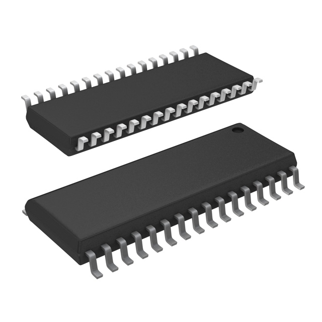
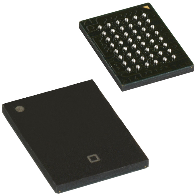
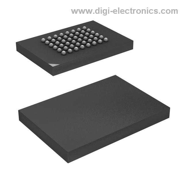
Packaging and Pinout Details of CY7C1079DV33-12BAXIT
The CY7C1079DV33-12BAXIT employs a highly compact 48-ball FBGA package, optimized for board space efficiency and advanced signal integrity. The package dimensions—8 × 9.5 × 1.2 mm—allow for dense system architectures without compromising electrical performance. Each ball position within the FBGA matrix is strategically assigned to facilitate direct and predictable signal routing, minimizing trace length and cross-talk while supporting high-speed data exchange. The pinout is engineered for versatility, with dedicated connections for both single and dual chip-enable configurations, streamlining the integration of either isolated memory subsystems or parallel memory banks on shared buses.
Non-connected (NC) balls are judiciously positioned to act as strategic layout buffers, enabling flexible PCB trace planning while retaining tight control over impedance. This approach also enhances reliability during multi-layer routing, accommodating complex stack-ups found in high-density assemblies. Such design allows seamless stacking of devices, expanding usable memory with minimal impact on board real estate—valuable in embedded platforms and IoT sensor hubs where physical footprint constraints are strict.
Compatibility across various interface scenarios has been embedded into the ball map itself, enabling the device to function as both a sole memory solution or part of a scalable array. Pin symmetry and corner alignment simplify automated placement and soldering processes, increasing yield in high-volume manufacturing. During reflow, the robust thermomechanical profile of the FBGA enclosure maintains solder integrity, reducing failure rates when compared to legacy TSOP or SOIC counterparts.
In practice, routing guidelines suggest favoring adjacent NC balls for ground pours or signal isolation, maximizing signal integrity—particularly in designs leveraging the dual chip-enable functionality for multiple independent address ranges. Fine pitch spacing supports reduced parasitic capacitance, a critical advantage when designing for faster memory access times. This deliberate balance between package density and electrical isolation is central to maintaining low noise floors in tightly integrated digital subsystems.
The adaptability of the CY7C1079DV33-12BAXIT’s packaging and pinout stands out through its robust support for custom memory configurations, allowing designers to scale performance or capacity with minimal redesign effort. Its FBGA layout represents not just a physical constraint solution but also an enabler for accelerated prototyping and rapid deployment into new product lines, giving engineering teams significant leverage in time-to-market-sensitive applications.
Timing, AC Characteristics, and Interface Considerations for CY7C1079DV33-12BAXIT
Timing analysis for the CY7C1079DV33-12BAXIT centers on its high-speed address to data access time ($t_{AA}$) of 12 ns. This parameter is crucial for designs targeting synchronous bus architectures exceeding 83 MHz, as it offers deterministic latency and facilitates pipeline stage allocation within advanced memory-mapped systems. In practice, maintaining timing integrity requires careful PCB trace layout to minimize propagation delays and reflections. Direct measurement of setup/hold windows reveals consistently tight margins embedded in the device specification, reducing the need for guard-band strategies in time-critical applications.
AC characterization adheres to industry-standard test vectors: input transition times capped at 3 ns and reference voltages anchored at 1.5 V. By aligning with common TTL and CMOS logic thresholds, the device ensures compatibility across diverse controller topologies. The provided timing diagrams delineate both read and write phases, enabling designers to synthesize timing constraints in VHDL- or Verilog-based workflows without recasting signal conventions. Layering timing abstraction over real-world measurements often exposes vulnerabilities in interface adaptation, particularly during edge rate mismatch between controllers and memory devices—a challenge mitigated here by robust signal envelope management.
Flexibility in system integration is afforded by dual cycle architectures; both chip enable– and write enable–driven protocols are supported. This duality streamlines design convergence where FPGA synthesized controllers require granular memory access arbitration, or microcontroller buses leverage asynchronous transaction models. Empirical bus validation demonstrates that the device responds predictably to both active-low gating and pulse-driven overwrite events, accommodating state machines that interleave read/write cycles with minimal cross-talk.
Output handling is engineered for dynamic bus environments. When deselected or during write operations, the device transitions outputs to high-impedance, preventing contention in multi-master systems and facilitating seamless bus sharing—integral for designs scaling beyond single-node memory access. This isolation is consistently observable during protocol sniffing sessions in shared SPI and parallel bus environments, where clear open-drain intervals validate the electrical isolation required for distributed memory topologies. The implicit prioritization of signal isolation ensures deterministic system behavior under load, preserving transaction throughput in dense bus architectures.
A subtle yet frequently overlooked advantage arises from the device’s predictable IO characteristics. The alignment of AC performance and tri-state output logic directly informs timing closure across asynchronous domains, where metastability or race conditions can emerge. Leveraging deterministic transition windows and high-impedance intervals enables refined timing constraint extraction, yielding resilience against signal skew and protocol violations—often a bottleneck in high-density memory controller implementations. This approach fosters scalable interface design, positioning the device as a foundational element in robust, timing-critical embedded systems.
Data Retention and Low Power Operation in CY7C1079DV33-12BAXIT
The CY7C1079DV33-12BAXIT leverages SRAM cell architecture to deliver robust data retention capabilities, which become vital in embedded platforms where supply voltage fluctuations and stringent power budgets are common. By supporting data retention down to 2.0 V, the device preserves cell state reliability even as the system enters deep standby. This voltage threshold is achieved through precise silicon process control and adaptive biasing within the memory cell design, ensuring charge integrity in the storage node despite reduced drive strength and leakage current risks at lower voltages.
System-level implementation benefits from this feature, as it permits seamless transition to low-power modes. The hardware-based power-down logic within the device actively monitors control signals and supply rails to autonomously enter retention mode without the need for complex external sequencing. When transitioning, peripheral circuitry is disconnected or clock-gated, reducing unnecessary toggling and static current draw while the memory core remains fully data-preserving. This approach aligns with best practices for achieving microampere-range standby currents in battery-backed and portable applications, extending operational life and maintaining system integrity during standby or brownout scenarios.
From a design perspective, integrating the CY7C1079DV33-12BAXIT within energy-constrained systems such as data loggers, industrial controllers, or wearable platforms simplifies power management architecture. The absence of external hold-up capacitors or dedicated retention supply rails reduces component count and PCB complexity. Furthermore, SRAMs with poor retention performance under low voltage can manifest as latent field failures or intermittent boot issues; this device mitigates such risks by guaranteeing bit stability to the specified threshold.
Applying these characteristics effectively requires careful PCB layout, particularly around supply decoupling and ground return paths to prevent transient undershoots below the retention voltage. Additionally, the interaction between memory retention and system wakeup protocols must be considered, as rapid VDD restoration is required to ensure seamless re-entry into active operation without partial data corruption. In scenarios demanding aggressive power cycling, the deterministic retention behavior streamlines validation testing and supports robust firmware design, eliminating the need for complex data restoration procedures on each wake-up.
Given these mechanisms, the CY7C1079DV33-12BAXIT not only supports the explicit needs of low-power system design but fundamentally enables a more reliable and scalable architecture for embedded developers navigating the tradeoffs between power efficiency, data integrity, and operational lifespan.
Potential Equivalent/Replacement Models for CY7C1079DV33-12BAXIT
Identifying suitable alternatives to the CY7C1079DV33-12BAXIT centers on scrutinizing core electrical and mechanical parameters to minimize the risk of performance degradation or unexpected system side effects. At the foundational level, focus falls on matching the essential specifications: memory density (32 Mbit), parallel data width (×8 organization), fast access time (no greater than 12 ns), and single-voltage operation at 3.3 V. Encapsulation in BGA packages, as dictated by the original footprint, governs the physical interchangeability and influences subsequent board-level reliability.
The broader CY7C1079DV33 family, including variants with diverse speed grades or chip-enable features, often serves as the initial substitution path. Within this product line, minor variations in standby current, output drive strength, or input threshold may impact designs with stringent power integrity or signal margin requirements—especially in noise-sensitive or battery-backed domains. Careful cross-examination of standby/leakage metrics ensures that silent upgrades do not incrementally erode power budgets, a critical consideration for IoT or industrial edge applications.
In parallel, examining peer offerings from SRAM leaders such as Renesas, Alliance Memory, or ISSI enables deliberate cross-brand sourcing strategies. Here, matching the datasheet specifications is only the first gate. Crucial secondary characteristics—including bus turnaround times, data retention levels below 2 V, and robust ESD/latch-up immunity—often surface as key differentiators during pre-qualification. For example, certain manufacturers incorporate deeper internal ECC or reinforced I/O clamp circuitry, which can translate to greater long-term system margin under electrically harsh operating conditions or during hot-swap procedures.
Transitioning to practical aspects, empirical board-level A/B swaps reveal that nominal spec matches do not guarantee seamless integration; subtleties such as input capacitance mismatches can affect edge rates and EMI behavior, sometimes mandating minor layout tweaks or firmware adjustments to maintain timing closure. In time-critical or synchronous memory interfaces, even slight deviations in tRC or output hold (tOH) require careful margin analysis, with oscilloscope validation across temperature extremes to safeguard against corner-case failures.
Best-in-class component qualification relies on more than datasheet conformance; robust projects establish a comprehensive test matrix encompassing worst-case timing, functional test patterns, and power-on sequencing. In high-availability automation or defense systems, dual-sourcing strategies increasingly favor parts with extended process longevity and published obsolescence notices to reduce field repair risk and lifecycle management overhead.
In summary, the pursuit of true drop-in replacements for the CY7C1079DV33-12BAXIT calls for rigorous technical due diligence. Direct electrical and mechanical compatibility aligns the substitution with legacy constraints, yet nuanced behavioral differences demand close scrutiny during validation. Sustained design resilience emerges from coupling meticulous compatibility assessments with real-world evaluation, ultimately supporting both immediate continuity and longer-term sourcing flexibility.
Conclusion
The CY7C1079DV33-12BAXIT is architected to address the stringent demands of high-performance parallel-access memory systems, commonly encountered in industrial controls, communication equipment, and embedded platforms. At its core, the synchronous static RAM (SRAM) fabric provides deterministic access timing, ensuring minimal latency and predictable operation crucial for real-time processing pipelines or latency-sensitive control loops. The device’s fast access cycles, typically in the sub-15ns range, align well with modern microprocessors and FPGAs that require rapid memory transactions to maintain throughput integrity.
Electrically, the chip supports robust voltage tolerances within the 3.3V interface domain, integrating power-down data retention mechanisms that safeguard against unintended data loss during brown-outs or unplanned resets. These retention features are vital in embedded deployments where power supplies are unregulated or shut down dynamically to extend operational life. The dual chip-enable capability enables flexible memory mapping and bank switching, which facilitates seamless expansion in designs with variable address ranges or time-multiplexed data flows.
When integrating the CY7C1079DV33-12BAXIT, attention to bus loading and signal timing is critical. Deployment experience highlights the importance of matching decoupling network design to the chip’s switching profile to suppress ground bounce during burst accesses. Peripheral timing analysis should factor in trace lengths and impedance to mitigate signal skew, which is especially relevant in high-noise environments or multi-board assemblies. Ensuring voltage compatibility across all interfacing components streamlines signal integrity and extends mean-time-between-failures, a decisive parameter in long-lifecycle equipment such as telecom infrastructure or industrial robotics.
From a system architecture perspective, the deterministic SRAM behavior presents a noteworthy advantage over cache-dependent volatile memory, removing the complexities associated with cache coherence and unpredictability. This characteristic simplifies application-layer software and hardware debugging, minimizing critical path variations and enabling more bounded worst-case execution time estimates.
Availability and continuity of supply further reinforce the practical suitability of the CY7C1079DV33-12BAXIT for long-term projects. Its established production track record and vendor support streamline procurement risk analysis and lifecycle management planning. Unlike commodity memory alternatives subject to rapid obsolescence, this part’s documentation stability and multi-sourcing potential offer an embedded reliability advantage, supporting qualification for safety-critical or certified systems.
Selection of the CY7C1079DV33-12BAXIT should rest on a holistic evaluation of timing requirements, electrical environments, scalability plans, and lifecycle constraints. Its technical features, seasoned real-world performance, and predictable supply underwrite its relevance for engineering teams seeking to de-risk critical memory subsystems within advanced digital designs.