>
>


Product Overview: CG8634AM Infineon Technologies PSoC 4100 MCU
The CG8634AM microcontroller, part of Infineon Technologies’ PSoC 4100 family, leverages an ARM Cortex-M0 core running at up to 24 MHz to deliver a low-power yet capable processing platform tailored for cost-sensitive embedded applications. The integration of 32KB flash and 4KB SRAM provides sufficient memory for contemporary control logic and real-time operations without imposing significant power or board area overhead. The MCU’s distinctive strength lies in its programmable analog and digital blocks, which can be reconfigured dynamically, enabling on-the-fly adaptation to diverse application demands. This granularity supports mixed-signal designs, allowing developers to integrate custom sensors, communication protocols, or HMI functionalities directly on chip, minimizing reliance on external components.
Underlying this architecture is a modular approach: analog blocks include comparators, ADCs, and opamps that may be routed flexibly via the internal analog matrix. Digital blocks enable logic operations, timers, PWMs, and communication interfaces, further augmented by a versatile GPIO subsystem. Such hardware abstraction removes traditional bottlenecks in pin routing and resource allocation, allowing firmware engineers to refactor and scale solutions without redesigning the PCB. In practice, this proves especially valuable in iterative product development, where pinout or peripheral requirements evolve late in the design cycle. The compatibility upheld across the PSoC 4 lineup also ensures continuity; migration between variants for increased resources or cost reduction is streamlined, requiring minimal codebase or layout modifications.
When deployed in sensor-centric environments or HMI implementations, the CG8634AM’s fast wakeup times and low standby current facilitate extended battery life, an essential trait for remote or wearable devices. The tightly integrated development ecosystem, featuring graphical hardware configurators and code-generation tools, shortens prototyping iterations and increases hardware validation accuracy. Real-world deployments reveal notable gains in design efficiency: implementing complex touch interfaces or custom sensor front-ends can be achieved with minimal external circuitry, reducing both BOM cost and EMI susceptibility.
A distinct insight emerges from applications that interleave analog signal conditioning with digital control, such as motor drivers or environment monitoring nodes. The MCU’s configurability empowers designers to prototype, test, and mass-produce with the same silicon, shifting the differentiation focus from hardware to firmware. Such flexibility not only accelerates time-to-market but also future-proofs product lines against evolving interface standards or changing user requirements. The combined effect of scalable pin multiplexing, robust mixed-signal integration, and cross-family compatibility marks the CG8634AM as a compelling choice for embedded architects seeking to balance cost, performance, and rapid adaptability within their system designs.
Architectural Highlights and Core Features of CG8634AM
The CG8634AM’s architectural foundation is centered on a 24 MHz ARM Cortex-M0 processor, emphasizing energy efficiency and computational capability. This is achieved through aggressive clock gating, which systematically deactivates inactive logic domains, thereby reducing both dynamic and leakage power. The core employs the Thumb-2 instruction set, allowing dense code execution while maintaining upward binary compatibility. This ensures a smooth upgrade path for applications that may transition to Cortex-M3, M4, or higher families, simplifying codebase maintenance in long-term deployment projects.
A standout feature is the single-cycle hardware multiplier, which proves instrumental when implementing digital filters, control loops, or cryptographic primitives where low-latency multiply-accumulate operations are paramount. Coupled with a sophisticated Nested Vectored Interrupt Controller (NVIC), the processor can dynamically prioritize up to 32 interrupt sources. The inclusion of a Wakeup Interrupt Controller further enhances responsiveness, as the device can rapidly transition from deep-sleep states with minimal latency—vital in real-time sensing environments or battery-powered nodes.
Memory subsystem innovations are evident in the flash architecture. The Read Accelerator enables zero wait-state fetches across the full 24 MHz frequency range, eliminating pipeline stalls and maximizing code throughput. Multiple flash protection schemes, spanning Open, Protected, and Kill modes, offer granular control over memory visibility and in-field code integrity. These security primitives are particularly valued in applications requiring firmware over-the-air updates or third-party code provisioning where selective debug access must be granted or revoked. Secure boot sequences and anti-tamper protocols can be constructed natively, leveraging these attributes without external circuitry.
On-chip debug support is realized through Serial Wire Debug (SWD), a streamlined two-pin interface that minimizes PCB routing complexity. Integrated breakpoint and watchpoint logic—four breakpoint and two watchpoint comparators—enables local and non-intrusive monitoring of execution in-situ. This facilitates iterative firmware refinement and aggressive fault analysis, even after the PCB has been fully assembled. The benefit extends to accelerated field servicing, since device introspection can proceed without board disassembly or intrusive probing.
In terms of system memory, the combination of 32KB embedded flash and 4KB SRAM addresses a broad spectrum of control-oriented and real-time applications. The SRAM is always-retentive through Hibernate mode, maintaining context and critical variables, which enables deterministic wake-up behavior and shortens warm-start periods in power-managed IoT deployments. The balance between program storage and working memory is well-suited for compact RTOS implementations, field protocol stacks, and integrated motor or power control loops.
Application experiences demonstrate that the CG8634AM’s architectural choices yield streamlined product bring-up, especially in low-energy sensor networks and secure node controllers. For instance, fast interrupt response and clocked flash reads have enabled precise pulse capture and on-the-fly signal analysis in industrial sensing modules. Similarly, the layered approach to memory security aligns with automotive and medical device requirements where code provenance and IP isolation are mandated. These observations reinforce a key viewpoint: the blend of CPU efficiency, memory versatility, and intrinsic security mechanisms collectively reduce risk and integration overhead for advanced embedded designs, making the CG8634AM a targeted solution for developers seeking both reliability and lifecycle scalability.
Analog and Digital Peripheral Resources in CG8634AM
Analog and digital peripheral resources distinguish the CG8634AM as a highly adaptable mixed-signal microcontroller, directly serving the requirements of precision-embedded designs. The synergy of these subsystems supports complex real-world interactivity, minimizing the typical reliance on external components.
The analog subsystem’s dual reconfigurable operational amplifiers provide a robust signal chain backbone. These opamps enable seamless implementation of programmable gain amplifiers, active filters, and low-impedance buffer stages, substantially simplifying schematic design and board-level routing. High drive capability supports direct interfacing with demanding sensor outputs or actuators, and the internal routing options limit parasitic noise. Configurability allows rapid transitions between signal conditioning, current sensing, and feedback applications without hardware changes, accelerating iterative development cycles.
The embedded 12-bit 806 ksps SAR ADC, with an intelligent channel sequencer, delivers reliable conversion for both single-ended and differential inputs. This mechanism enables consolidated acquisition from arrays of sensors or mixed-voltage domains. Accuracy remains consistent across varied acquisition scenarios due to flexible internal and external reference selections, and the sequencer streamlines multipoint calibration or background monitoring tasks typical in distributed sensing networks.
Integrated current DACs extend analog functionality by supplying programmable bias currents, critical for resistive sensor excitation, charge-pump generation, or capacitive sensing front-ends. By pairing IDAC outputs with on-chip comparators, fast analog event detection or custom touch/proximity interfaces are implemented without firmware latency or excessive power drain. Comparators feature ultra-low operating current, sustaining system vigilance throughout deep sleep and hibernation states—vital for battery-dependent or always-on designs, where continuous voltage supervision and threshold detection replace discrete analog watchdog ICs.
Thermal management and calibration come standard through the integrated temperature sensor, presenting real-time silicon junction thermal data. Digitization through the onboard SAR ADC provides frictionless access for slope compensation, gain-tracking, or dynamic environmental adaptation, creating opportunities for closed-loop analog compensation directly on-chip.
On the digital front, dual Serial Communication Blocks (SCBs) offer extensive protocol agility. Each block is multiplexed between I²C, SPI, or UART operation, supporting standard and legacy interfaces without silicon substitution. Features such as LIN, IrDA, and Smartcard support—alongside hardware FIFOs—expand utility into domains ranging from industrial control to secure authentication and legacy device bridging. Multi-protocol operation facilitates migration between designs and quick adaptation to evolving system requirements. High I²C bus rates, coupled with clock stretching and multi-master arbitration, secure robust interconnectivity even on congested buses.
The four flexible 16-bit Timer/Counter/PWM blocks support variable-duty and dead-time insertion modes. Such features are indispensable in actuator management, closed-loop control, and power electronics, permitting custom PWM patterns for brushless DC motors, solenoids, or lighting dimming—all without software-side cycle stealing. Edge and center-aligned generation, along with pseudo-random patterns, expand the signal modulation possibilities for EMI-sensitive or secure signaling environments.
Programmable combinatorial and sequential logic with a high-speed I/O matrix enables rapid hardware abstraction, moving application-specific control paths into the peripheral domain. This approach not only improves response latency, but also offloads processor intervention, resulting in higher deterministic throughput and greater firmware modularity.
A distinctive aspect of CG8634AM lies in its software-driven configurability. PSoC Creator design tools orchestrate peripheral setup as reusable, application-defined hardware functions—shortening development cycles and supporting late-stage design pivots. Adapting analog and digital blocks in firmware, rather than relying on static silicon allocations, creates intrinsic hardware reuse across successive projects. This capability unlocks advanced mixed-signal integration without PCB revisions, fostering a platform approach in product engineering.
The convergence of these tightly coupled analog and digital elements delivers practical advantages: minimal BOM, streamlined EMI management, and simplified pin multiplexing. Yet, its true strength becomes apparent in rapid prototyping and scalable manufacturing scenarios, where differentiated interfacing, closed-loop control, and multi-domain signal processing deliver tangible, competitive engineering value.
Power, Clocking, and Low Power Operation in CG8634AM
Power distribution and clocking mechanisms in the CG8634AM are optimized for energy-centric deployment, particularly where dynamic supply configurations intersect with stringent power budgets. Direct single-supply compatibility across a broad voltage range (1.71V to 5.5V) enables seamless integration into platforms sourced either from primary cell stacks or fine-grained regulated rails. This architectural latitude not only streamlines PCB design, reducing level-shifter overhead, but also allows for aggressive battery sizing in mobile and sensor node applications.
Power management is engineered around granular state control, leveraging hardware transitions between Active, Sleep, Deep Sleep, Hibernate, and Stop modes. The Stop Mode curtails leakages to sub-20 nA, chiefly through selective power-gating and retention of edge-critical resources like GPIOs for event-based wakeup. Such event-driven recovery flows mitigate latency spikes after power collapse, promoting rapid return to operational eligibility in distributed sensing or intermittently powered systems. Experience shows that persistent brown-out detection (BOD) and autonomous power-on reset (POR) significantly enhance reliability—and minimize system deadlocks—when supply rails are subject to transients, such as during automotive engine cranking or industrial rapid cycling.
Clock subsystem flexibility is reflected in the dual oscillator strategy: the primary IMO, factory-trimmed to ±2% (3–24 MHz), and the secondary low-speed ILO for background operations. Selection and calibration of these oscillators can be dynamically orchestrated, balancing throughput requirements against energy profiles. The high-resolution clock divider matrix allows synchronous alignment of peripheral blocks, including ADCs or communication interfaces, with modulated frequencies to reduce crosstalk and power spikes under concurrent activity. Experience has indicated that careful divider staging during multi-peripheral polling cycles directly influences system-level noise reduction and EMI resilience, a must when deploying in mixed-signal environments.
Precision analog conversion hinges on selectable voltage reference sources. Internal options provide simplicity, while external reference bypass permits elevated signal-to-noise ratios and linearity—particularly critical in instrumentation scenarios or when integrating sensor suites demanding consistent offset calibration. Systems implementing external reference strategies consistently register tighter conversion spreads and lower drift across temperature cycles.
These architectural features coalesce to enable robust hardware adaptation across varying industry domains. The modular power and clocking frameworks, coupled with precise reset and reference subsystems, support aggressive energy harvesting, stringent uptime requirements, and reliable operation in environments characterized by frequent supply volatility. Implicitly, the CG8634AM’s design signals a shift towards deeply integrated power-state logic and flexible clock architectures as foundational to next-generation low-power embedded systems.
I/O Capabilities and Package Options of CG8634AM
The CG8634AM presents an advanced I/O architecture tailored for demanding mixed-signal designs, delivering notable adaptability across hardware layers. At the core of its versatility are 36 fully programmable GPIOs. These pins provide comprehensive configurability, with support for analog signal acquisition, capacitive touch sensing via CapSense, LCD segment driving, and standard digital IO. Each GPIO pin features parameter tuning such as drive strength adjustment, threshold selection between CMOS and LVTTL standards, and individually assignable slew rates to mitigate electromagnetic interference. This per-pin customization ensures compatibility with diverse signal environments and enables precise impedance matching critical for sensor integration and EMI compliance.
The interrupt architecture further elevates the CG8634AM’s utility. By allowing independent interrupt sourcing from every pin, the device supports scalable sensor matrix and HMI implementations. This granular control over event triggers streamlines system-level firmware, reducing polling overhead and facilitating real-time response in safety-critical and user interface applications, such as large touch key arrays or multi-channel contact detection.
The embedded segment LCD controller operates with up to 4 common lines and 32 segment outputs. Driving methodologies include both digital correlation for crisp, stable display updates and PWM techniques that permit dynamic brightness modulation. These options harmonize display power usage and visibility, even during low-power system states, without sacrificing interface fidelity. Integration is direct, bypassing the need for optoelectronic drivers, which simplifies design and reduces BOM complexity.
CapSense functionality utilizes a Cypress-originated Sigma Delta (CSD) engine, reinforced by SmartSense™ automatic calibration. This eliminates manual iterative tuning by adaptively optimizing sensitivity and threshold parameters according to varying parasitic capacitance or environmental moisture. Engineers can confidently deploy capacitive touch controls on plastics, glass overlays, or in humid conditions, as the embedded algorithm reliably filters baseline drift and prevents false actuation—traits verified across prototype cycles involving irregular or contaminated touch surfaces without external tuning components.
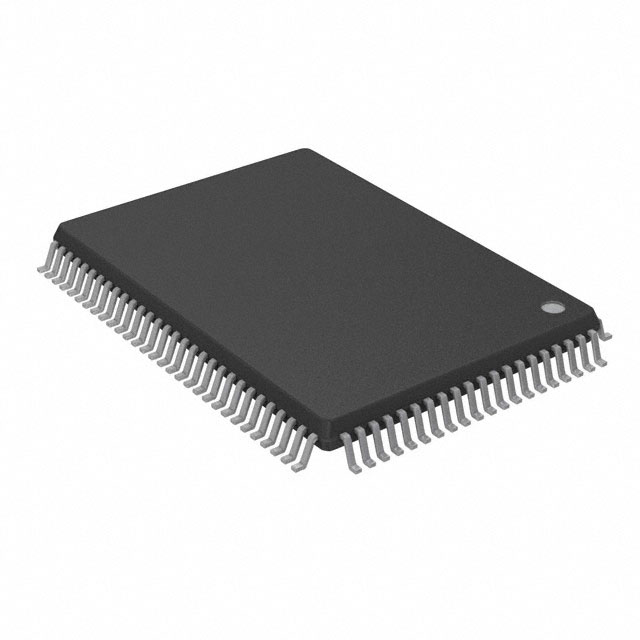
The package selections for the CG8634AM reflect the device’s application-conscious engineering. The 44-TQFP format (10x10 mm) combines a high pin count with straightforward PCB assembly. This footprint balances the trade-offs between solderability, board density, and cost, facilitating integration in mid-tier control modules, both in commercial appliances and industrial sensor hubs. The thermal characteristics and pin pitch also streamline automated placement and reflow, supporting stringent yield requirements and serviceability in production.
An integral design principle visible throughout the CG8634AM portfolio is its accommodation of complex, multi-modal embedded systems while maintaining operational simplicity. Layered configurability ensures each subsystem—from analog front-ends to interactive displays—coexists with minimal cross-coupling and predictable performance margins. Such architectural foresight accelerates time-to-prototype and expedites field adaptation, especially when developing products where a single microcontroller must orchestrate diverse interfaces under variable operating conditions. This engineering-centric focus, coupled with robust package support and mature sensing algorithms, positions the CG8634AM as a foundational choice for scalable, reliable interface solutions in next-generation smart devices.
Integrated Development Ecosystem for CG8634AM
The integrated development ecosystem supporting CG8634AM stands out for its comprehensive alignment of design, verification, and deployment capabilities, directly targeting streamlined engineering workflows. PSoC Creator, Infineon's flagship IDE, forms the backbone for rapid hardware/firmware co-design. Its graphical schematic capture abstracts complex analog and digital routing, allowing for simultaneous configuration and verification. The embedded library containing over a hundred pre-verified IP components accelerates architectural experimentation and system bring-up, eliminating the lengthy process traditionally associated with low-level peripheral validation. This configurability, combined with hierarchical design methods, enables scalable hardware abstraction—from board-level signal interconnection to block-level functional composition.
Integration with ARM-standard toolchains ensures developers can leverage pre-existing automated build, debug, and simulation infrastructures. Seamless compatibility facilitates code reuse across product iterations, reducing migration overhead and preserving legacy investment. Compilation, linking, and real-time debugging are unified under familiar environments, allowing for immediate bridging from prototype to production code without laborious transitions.
Supporting resources articulate subtle implementation details often glossed over in datasheets. Technical reference manuals delve into peripheral register-level operation, while application notes share solution patterns for signal conditioning, power management, and real-time control. Evaluation kits, notably the CY8CKIT-042, -049, and -001 series, offer modular hardware platforms that mirror real-world use cases, allowing instantiation of typical workloads—time-critical communication interfaces, precision analog measurement, or custom logic blocks. These platforms expedite empirical validation of design hypotheses and benchmarking under production-mimicking scenarios.
Production support mechanisms further distinguish the ecosystem’s maturity. In-system programming via SWD/JTAG provides a deterministic path from prototype firmware to field deployment, with robust debug interfaces that allow trace-level fault isolation. Bootloader-enabled packages support over-the-air firmware updates, minimizing downtime and simplifying update logistics in distributed systems.
Direct exposure to tightly integrated design flows yields observable reductions in error propagation between hardware and software domains. Iterative prototyping within this ecosystem consistently uncovers subtle corner cases early, promoting architectural resilience and lowering risk profiles as projects scale. The convergence of design abstraction, reference frameworks, and live debug instrumentation translates into accelerated design convergence and a flatter learning curve for multidisciplinary teams.
A crucial insight stems from the adaptability of the CG8634AM ecosystem: its vertical integration supports both exploratory prototyping and mature product realization on the same foundation. This modular architecture empowers incremental deployment of new features, rapid pivoting in response to changing specifications, and predictable control over project timelines. Opportunity cost is diminished not only by faster time-to-market, but also by sustained support for evolving design requirements. The ecosystem’s structure, emphasizing layered abstraction and rapid verification cycles, affirms its value for engineering-driven organizations seeking reliability without sacrificing agility.
Electrical and Thermal Specifications of CG8634AM
Electrical and thermal specifications of the CG8634AM demonstrate a decisive commitment to operational robustness across challenging application domains. The device guarantees reliable function over an extended temperature range from –40°C to +105°C. This operational envelope directly aligns with stringent requirements in both industrial and automotive contexts, where devices must uphold consistent performance despite wide external temperature excursions and frequent thermal cycling. The broad thermal tolerance ensures that system designers can implement the CG8634AM in environments with unpredictable conditions, minimizing derating needs and extending service life, even in tightly packed modules subject to rapid heating or cooling.
The electrical specification profile is engineered for deterministic behavior throughout the full supply voltage range of 1.71V to 5.5V. This wide supply margin allows flexible power architectures, including direct battery attachment or operation from regulated supplies in noisy industrial settings. Ensuring that DC and AC characteristics hold within the specified limits over the entire voltage and temperature space, the CG8634AM offers designers repeatable timing for core logic, peripheral modules, and I/O interfaces under all operating scenarios. This level of predictability eliminates the need for margin-heavy guard bands in timing analysis, supporting aggressive design closure in safety- or performance-critical embedded applications.
Peripheral blocks such as the ADC, opamp, comparator, and digital serial interfaces (UART/SPI/I²C) feature explicit parameterization for offset, gain, linearity, setup/hold times, and drive strengths. Such granularity enables direct modeling within electronic design automation (EDA) environments, enhancing simulation accuracy for analog front ends and data communication links. GPIOs, with deterministic switching thresholds and drive capabilities, mitigate risk in interconnected systems by enabling thorough pre-layout signal integrity and timing budget assessment. This approach supports high interconnect density on PCBs, improving EMI/EMC compliance without requiring time-intensive empirical tuning post-layout.
Package definitions strictly adhere to JEDEC standards, with moisture sensitivity levels clearly demarcated. This provides clear guidance for manufacturers regarding pick-and-place handling, storage, and reflow profiles. Standardized outlines accelerate multi-sourcing viability, which is a key consideration for risk-averse supply chain strategies. By embracing industry-accepted moisture sensitivity ratings, the CG8634AM allows seamless inclusion in automated assembly processes and aligns with quality assurance protocols widely deployed in high-volume production lines.
A defining insight in the CG8634AM specification is the meticulous alignment of parametric guarantees with system-level engineering needs. Rather than relying solely on typical values, the device’s characterization reflects worst-case analysis—a methodological choice that directly supports robust design-for-reliability strategies. When implemented in real-world systems, these practices reduce late-stage design iterations caused by field reliability escapes and facilitate first-pass success, especially in certifications for functional safety or mission-critical platforms. This union of comprehensive, transparent technical detail and process-friendly integration features positions the CG8634AM as a pragmatic selection for modern embedded system design.
Potential Equivalent/Replacement Models for CG8634AM
Evaluating potential equivalents or replacements for the CG8634AM within the Infineon (formerly Cypress) PSoC 4 ecosystem demands a methodical comparison anchored in both hardware capabilities and design constraints. A thorough assessment starts with understanding the architecture’s modularity, where variations in flash memory, SRAM, and pin count across the PSoC 4100 family establish foundational scalability. Devices ranging from compact 28-pin SSOP to versatile 48-pin TQFP cater to diverse PCB layouts, facilitating design continuity or enabling transitions to more complex systems without excessive board rework.
Examining upward compatibility, the PSoC 4200 series significantly increases computational headroom. These variants integrate higher-frequency cores and richer analog/digital peripherals, streamlining both signal acquisition and processing tasks that exceed the CG8634AM’s base capabilities. Such enhancements directly support performance-centric deployments, including multi-sensor management and advanced communication protocols. Migrating to the 4200 series often preserves peripheral mapping, simplifying firmware adaptation while leveraging improved efficiency and throughput.
On the other hand, scenarios emphasizing stringent cost control or minimal analog peripheral utilization can benefit from the PSoC 4000 family. These models pare down feature sets and resources to optimize unit pricing, maintaining functional adequacy for less demanding applications such as basic motor control or interface bridging. Furthermore, low-power operational features in 4000/4100 variants enable energy-sensitive products in both battery-powered and always-on use cases, presenting practical advantages during long-term field operation.
The nuanced process of model selection pivots on matching package constraints—whether dictated by mechanical enclosure, automated assembly limitations, or spatial density—to available datasheets. Analog channel requirements further delineate compatibility, especially in multi-sensor or precision control domains, where scalable op-amp, ADC, or DAC resources minimize external BOM complexity. Communication flexibility via built-in support for I²C, SPI, or UART fosters direct interconnect compatibility, reducing integration effort for third-party modules.
Historically, iterative migration exercises have shown that careful peripheral mapping and memory budgeting minimizes firmware redesign effort. By starting with detailed pinout matrices and identifying peripheral mismatches early, development cycles compress significantly, particularly when leveraging Infineon’s unified toolchains. Power profiling across candidate models is best integrated at the prototyping phase, where real-world consumption figures often differ materially from nominal datasheet values. Attention to errata documentation and peripheral quirks also streamlines later-stage testing, insulating production runs from unexpected edge cases.
In practice, prioritizing forward scalability—such as selecting devices with surplus memory or reserving analog features—provides a hedge against future feature creep or variant expansion, often outperforming short-term cost optimization. Strategic selection thereby enables a more resilient product roadmap, with layered architecture permitting both vertical (feature-rich) and horizontal (cost-optimized) platform extension across generations. Such an approach inherently supports smoother migration and reduced risk exposure in dynamic sourcing environments.
Conclusion
Engineering evaluation of the CG8634AM MCU centers on its layered architectural flexibility and analog/digital integration, which distinguish it among competing single-chip solutions. Powered by an ARM Cortex-M0 core, the device achieves a balance between computational throughput and low power consumption, making it optimal for designs constrained by thermal and energy budgets. This is critical where stand-alone MCUs previously presented fixed peripheral sets or limited analog configurability, leading to repeated board respins in evolving application spaces.
The strength of CG8634AM lies in its fine-grained analog subsystem, allowing programmable routing between ADCs, DACs, and comparators. This enables rapid prototype adaptation and system calibration. In practice, projects spanning industrial control, sensor interface, and capacitive touch panels benefit from the MCU's support for field-reconfigurable analog blocks, which effectively compress BOM complexity and reduce time-to-market. Such integration allows engineers to consolidate discrete components—signal conditioning, filtering, voltage measurement—on-chip, lowering PCB area and simplifying validation cycles.
A key mechanism supporting agile engineering workflows is advanced peripheral configuration via PSoC Creator and compatibility with Eclipse-based toolchains. This setup streamlines firmware development and peripheral pin-mapping, allowing incremental hardware feature redefinition without invasive layout changes. The ability to leverage user-defined hardware functions on top of standardized digital and analog resources enables adaptation to highly variable market requirements, especially when user interface modalities or sensor sets shift late in the design phase. On multiple occasions, leveraging the dynamic reconfigurable matrix has mitigated the risk associated with mid-project specification updates.
Design teams operating in cost-sensitive contexts benefit from the MCU’s scalability and memory footprints. It is positioned for both entry-level and advanced designs, with upward compatibility for existing PSoC installations. The programmable nature of the device supports functional consolidation and obsolescence management, especially beneficial when legacy subsystems transition to modern workflows or when cost containment targets limit component proliferation. Migration from fixed-function MCUs is facilitated by the onboard peripheral flexibility, reducing both the firmware and hardware overhead typically mandated by global product variants.
In legacy system upgrades and greenfield deployments alike, the CG8634AM’s architecture allows real-time resource allocation adjustment, essential for long-term support and feature enhancement. Its built-in analog precision and digital configurability merge with industry-standard toolchain alignment, fostering a robust ecosystem for collaborative development and simplified cross-team asset sharing. On reflection, the device’s key advantage is its native capacity for in-field feature extension—unlocking new application spaces without disruptive hardware redesign. For dynamic embedded programs where adaptability, cost constraints, and time-to-market are tightly coupled, this platform offers distinct advantages in reliability and project agility.