>
>


Product overview: AD7623ASTZ Analog Devices 16-Bit SAR ADC
The AD7623ASTZ exemplifies high-performance analog-to-digital conversion through its robust successive approximation register (SAR) architecture, delivering 16-bit resolution at a throughput of 1.33 MSPS. At the core, the SAR approach leverages a binary search algorithm, rapidly narrowing the analog input to its digital equivalence within a set number of comparison cycles. This deterministic conversion sequence ensures minimal latency and exceptional repeatability, which is paramount in feedback control systems where signal integrity and timing are critical.
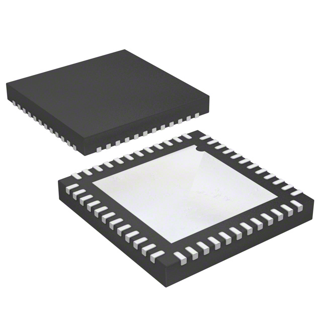
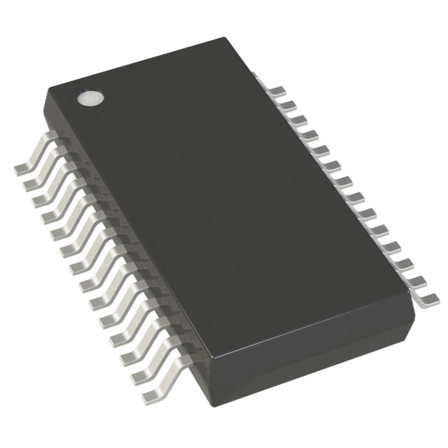
Integrated into a compact 48-lead LQFP or LFCSP_VQ package, the AD7623ASTZ offers significant board space savings without sacrificing analog performance. Its true differential input structure underlies superior common-mode rejection, effectively curbing susceptibility to ground potential differences or electromagnetic interference—a frequent challenge in industrial and test environments. This input design also promotes direct interface with differential sensors and signal conditioners, circumventing preamplification stages and thus reducing system complexity and noise ingress.
The device’s optimized power profile supports deployment in portable or thermally constrained instrumentation. Power scales with throughput, maintaining conversion accuracy even in low-power modes. Designers notice that the device’s efficient conversion engine and integrated reference buffer minimize drift and thermal-induced offset, reinforcing measurement stability across extended sessions or fluctuating ambient conditions.
Noise performance is engineered for applications requiring reliable sub-LSB accuracy. The 16-bit quantization makes the AD7623ASTZ suitable for digitizing small dynamic signals in data acquisition modules, scientific instrumentation, and medical electronics. In rigorous calibration routines or adaptive sampling systems, the ADC’s fast settling time and low glitch energy facilitate precise signal tracking during rapid input changes.
A distinguishing feature is its flexibility in both serial and parallel data interfacing. High-speed parallel output allows straightforward integration into FPGA-based acquisition chains, eliminating bottlenecks in multichannel architectures. When board real estate or pin count must be minimized, the serial SPI-compatible output provides seamless connectivity at no significant increase in system overhead.
Deployment experience indicates the importance of meticulous layout and reference circuitry selection. Proper decoupling at the supply and reference pins prevents signal degradation due to digital clock feedthrough or ground bounce, crucial when co-locating multiple high-resolution ADCs. The combination of differential inputs and efficient conversion logic mitigates channel-to-channel crosstalk, allowing dense sensor arrays or multiplexed measurement stages without performance compromise.
Overall hardware integration demonstrates that the AD7623ASTZ’s SAR core, low-power operation, and advanced input topology collectively streamline demanding data acquisition projects. Its architecture aligns with stringent application needs such as power grid monitoring, process automation, and waveform digitization within precision laboratories. The combination of deterministic sampling, versatile interfacing, and immunity to ambient noise positions the AD7623ASTZ as a foundational element for systems driven by both reliability and measurement integrity.
Key features and performance specifications of the AD7623ASTZ
The AD7623ASTZ is engineered to address the stringent demands of precision, speed, and integration in data acquisition systems. At its core, the SAR ADC architecture enables a true no-latency conversion cycle, providing a throughput of 1.33 MSPS without pipeline delay. This mechanism is fundamental for applications where sample-to-output latency directly impacts system performance, such as in closed-loop control or multiplexed sensor arrays. The absence of pipeline delays ensures deterministic response times, which is a critical parameter in high-speed instrumentation and emerging edge data-processing use cases.
Precision is realized through 16-bit resolution maintained by guaranteed no-missing codes, and a typical integral nonlinearity of ±1 LSB. This degree of linearity supports accurate sensing across the converter's dynamic input range, reducing the need for elaborate digital correction algorithms downstream. Combined with a SINAD of 88 dB and THD of -97 dB, the AD7623ASTZ provides a clean signal chain, suitable for vibration analysis, spectral monitoring, and precision servo feedback systems. These metrics are achieved not only under typical conditions but are robust against supply variance and temperature drift, enabled by the integrated, low-drift voltage reference and temperature sensor. This removes external reference dependencies and improves system calibration stability over life.
Power efficiency is integral to the device's design. Operating at a typical 45 mW at maximum throughput and scaling down at lower sampling rates, the AD7623ASTZ allows for deployment in portable or thermally constrained instrumentation without sacrificing conversion speed. The internal architecture actively manages power modes, reducing unnecessary consumption in idle or low-traffic phases—a frequently overlooked advantage when balancing acquisition performance with infrastructure limitations. The single 2.5 V core supply streamlines system power architecture, further reducing external component count, cost, and board complexity.
Flexibility in interface and integration is paramount for modern embedded designs. The AD7623ASTZ's digital I/O operates from 2.3 V to 5.25 V, offering broad compatibility with a mixture of legacy processors and current low-voltage FPGAs or MCUs. Engineers benefit from selectable parallel or serial digital communication—supporting industry-standard protocols such as SPI, QSPI, MICROWIRE, and DSP-specific interfaces. This reduces migration friction in platform upgrades and allows tighter integration in modular system designs. Pin-compatibility with the AD7677 series ensures a seamless upgrade path for legacy designs, minimizing redesign effort and mitigating supply chain risks in long product life cycles.
The differential input range of ±VREF enables optimal utilization of the ADC’s full-scale range and enhances immunity to common-mode noise—a necessity in harsh environments or long analog signal runs. The option of using the accurate internal reference or an external source gives designers granularity to tailor noise performance or system-wide synchronization schemes. In practice, selecting the internal reference offers the lowest drift and best match to the ADC core, while external referencing provides flexibility for multi-ADC array synchronization.
From a system perspective, the AD7623ASTZ functions as a signal fidelity enabler in medical imaging, industrial automation, and test and measurement instrumentation. Its feature set aligns with applications requiring both rapid acquisition and uncompromised linearity, including multi-channel data loggers, motor drive diagnostics, and real-time spectrum analyzers. Field experience demonstrates that appropriate layout, robust grounding, and careful power-supply decoupling further enhance the already strong noise immunity and simplify EMC certification processes. Strategically employing track-and-hold front ends can maximize the SAR ADC’s efficiency in rapidly changing signal environments.
An inherent yet often underutilized capability is the device’s adaptability for system self-monitoring and on-site recalibration workflows, leveraging the built-in temperature sensor data and reference monitoring. This enables predictive maintenance routines and higher system uptime in deployed assets.
In synthesis, the AD7623ASTZ encapsulates the key requirements for modern data capture: fast, precise, and flexible operation, delivered with engineering-centric features that mitigate historical compromises between speed, power, and integration. Its architecture, interface options, and upgrade path reflect a forward-looking design philosophy—preparing systems for both current requirements and scalable expansion as application complexity increases.
Applications suited for the AD7623ASTZ
The AD7623ASTZ, with its combination of high sampling rates, 16-bit resolution, and low power consumption, is well-aligned for demanding analog-to-digital conversion tasks across several engineering domains. Its SAR (successive approximation register) architecture ensures deterministic latency and robust performance in time-critical applications. Precision and throughput define its core utility: this converter reliably captures rapidly changing analog signals without sacrificing measurement fidelity.
In medical instrumentation, the AD7623ASTZ addresses the stringent requirements of equipment such as ECG, EEG, and other diagnostic monitors. These systems depend on low-noise, high-resolution conversions to detect subtle physiological signal changes. The device’s low input bias current and high dynamic range enable accurate digitization of microvolt-level signals, particularly advantageous in electrically noisy hospital environments where interference suppression and reliable isolation of true biomedical signals are critical.
Within high-speed data acquisition systems, the AD7623ASTZ’s ability to simultaneously sample multiple channels facilitates real-time data capture from sensor arrays or multiplexed inputs. An engineer setting up automated monitoring or control platforms benefits from the part’s inherent channel-to-channel consistency, minimized aperture jitter, and swift throughput, which are essential factors when synchronizing multi-source measurement streams or maintaining continuous, lossless logging.
Digital signal processing front-ends in communication systems often require converters that balance bandwidth with precision. Here, the AD7623ASTZ serves as a bridge between analog front-ends and DSP or FPGA cores, feeding finely digitized data without introducing unacceptable latency. This capability is critical in applications such as baseband I/Q demodulation or spectral monitoring, where phase coherence and amplitude linearity directly affect overall system performance.
Industrial instrumentation and spectrum analysis equipment leverage the device’s rapid conversion speed and precise integral nonlinearity to enable detailed parameter extraction from high-frequency or complex analog waveforms. When analyzing fast-changing industrial signals—such as vibration patterns in predictive maintenance or power quality waveforms—the converter’s consistent performance across temperature and supply ranges reduces calibration effort and long-term drift concerns.
Automated test equipment (ATE) platforms benefit from the AD7623ASTZ’s repeatability and fast recovery times during rapid signal switching. Its capacity to maintain accuracy under dynamic load conditions streamlines test workflows, increases throughput, and enhances measurement reliability—key attributes when characterizing semiconductor components, PCBs, or assembled systems under test.
Optimally leveraging the AD7623ASTZ in these roles involves nuanced PCB layout considerations to minimize crosstalk, careful power supply decoupling to suppress noise-induced errors, and sophisticated firmware for timing control and remote configuration. In practice, direct experience demonstrates the value of pairing the converter with low-drift voltage references and employing tight ground partitioning to support its theoretical performance in real-world settings. These considerations maximize both the immediate and long-term utility of the AD7623ASTZ within advanced, high-integrity electronic systems.
Detailed functional architecture and signal chain
The AD7623ASTZ employs a high-speed successive approximation register (SAR) ADC architecture, utilizing a capacitive digital-to-analog converter (DAC) for charge redistribution and supporting true differential input operation. This core mechanism provides precise analog sampling and conversion, anchored by tightly matched capacitor arrays that minimize gain and offset errors while providing superior common-mode rejection. Such an architecture ensures robust performance across varying operational environments, especially where noise and signal integrity are central design constraints.
The device integrates an internal sample-and-hold circuit tightly coupled to the input stage. This configuration securely captures the instantaneous analog input, isolating the core from upstream analog fluctuations that may disrupt conversion accuracy. The on-chip conversion clock synchronizes SAR cycling without demanding clock routing external to the device; this reduces layout complexity and mitigates timing skew, a vital benefit in high-channel-density systems. Further, the inclusion of an internal voltage reference and buffer standardizes input scaling and stability, decreasing susceptibility to external reference drift and thermal variances, thus supporting repeatable measurements over wide temperature ranges and operational lifetimes.
A digital error correction block operates in real time within the conversion chain. By mathematically analyzing comparator transitions during SAR operations, it compensates for capacitor mismatches, enhancing effective number of bits (ENOB) beyond what component tolerances alone would allow. This feature is vital in system-level applications where error budgets are tightly constrained and primary calibration opportunities are limited.
Selectable digital I/O interface modes accommodate both serial and parallel communications, optimizing data throughput and integration into heterogeneous backend architectures. The absence of pipeline latency is a direct result of the SAR approach—each digital code is finalized at the end of its respective conversion cycle, eliminating uncertainties in sample timing. In multi-channel, multiplexed scenarios such as automated test equipment or industrial control modules, this deterministic nature guarantees precise timing alignment between analog events and digital readouts.
Practical experience with the AD7623ASTZ signal chain reveals marked improvements in system synchronization when deploying the device within multiplexed analog front ends. The reduced external component count not only shortens bill-of-materials lists but also eases layout drafting, dampening parasitic influences in high-speed contexts. In particular, the differential input configuration exhibits strong resilience against ground loops and external interference, a recurring obstacle in harsh industrial settings.
A critical insight lies in the interaction between the charge redistribution DAC and the input buffer. The precise timing demanded by the internal SAR cycling mandates careful attention to driver bandwidth and settling performance upstream. Matching input driver impedance and minimizing kickback-induced settling error are essential for maintaining the stated accuracy and throughput, underscoring the advantage provided by the integrated sample-and-hold and reference buffers.
This layered, monolithic architecture—fusing analog, digital, and clock management domains—positions the AD7623ASTZ as a versatile node in signal acquisition pipelines, particularly where deterministic performance and low-latency conversion drive system objectives. By uniting these mechanisms, the device presents a compelling foundation for scalable data acquisition, blending analog precision with digital efficiency.
Analog input structure and driver amplifier considerations for the AD7623ASTZ
The analog input topology of the AD7623ASTZ centers on a true differential interface optimized for environments marked by pronounced electrical interference. This configuration leverages inherent common-mode rejection—substantially suppressing nuisance signals imposed uniformly on both inputs, such as transient disturbances commonly encountered in industrial automation racks or diagnostic imaging rails. With integrated ESD protection diodes positioned at the input nodes, vulnerability to high-energy spikes is mitigated. However, tolerance margins remain narrow; any excursion outside ±0.3 V from the designated supply rails risks diode conduction and potential performance compromise. Maintaining this headroom in field deployments requires careful PCB layout and supply sequencing, especially where plug-and-play sensor modules or float voltages are present.
The native input impedance, engineered to accommodate direct drive from low-output-impedance sources, supports straightforward interface with signal conditioning modules—yet, this simplicity does not obviate the need for deliberate driver selection in high-fidelity applications. The imperative to preserve AC performance, particularly under elevated throughput rates, arises from the interaction between the on-chip sample-and-hold circuit and the external driver’s dynamic output behavior. There, the acquisition time and slew rate of the driver stage become pivotal in maintaining low total harmonic distortion. Devices such as the AD8021, with bandwidth extending well beyond the conversion window and settling times below critical thresholds, consistently yield conversion linearity within 16-bit tolerances for full-scale transients. Extensive bench validation has shown that substituting the AD8021 with lower-performance amplifiers introduces subtle settling artifacts, notably when handling fast, multiplexed sensor arrays. Selecting from the AD8022 or AD829 portfolio allows engineers to tune noise performance, bandwidth, and quiescent power to system-level constraints—whether optimizing for low-voltage microcontroller interfacing or high-speed multiplexed channels.
Signal path integrity is further secured when interfacing unipolar voltage outputs sourced from precision sensors or DAC stages. Employing differential drivers such as the AD8139 provides an architecture for converting single-ended signals to a balanced, differential format. This conversion retains the noise immunity of the ADC’s native topology. By deploying simple RC filtering stages at the driver output, time-domain excursions and high-frequency noise are attenuated, and aliasing artifacts—particularly those exacerbated by undersampling in wideband measurement—are suppressed. Field experience highlights that judicious selection of R and C values, in accordance with input capacitance and conversion frequency, can yield marked improvements in SNR, even in installations with variable ground currents or nearby power switching events.
A subtle but consequential dimension emerges from the nuanced interaction between analog system impedance and ADC input structure. Source impedance above recommended ranges not only impairs settling but elevates susceptibility to signal droop during rapid sampling. In modular designs utilizing long signal chains, careful simulation and empirical measurement—prior to final assembly—have frequently revealed the need for compact buffer stages or local bypassing, especially where board-level crosstalk and distributed capacitance introduce unsuspected error terms.
The essential insight is that achieving optimal conversion in practical scenarios extends beyond textbook-matching of driver bandwidths—it mandates integrative attention to parasitic network effects, supply integrity, and nuanced amplifier settling dynamics. Direct, analytically informed component selection, paired with empirical validation under target operating conditions, consistently advances the robustness and precision of systems anchored by the AD7623ASTZ.
Reference voltage management in the AD7623ASTZ
Reference voltage management in the AD7623ASTZ centers on balancing internal convenience with external flexibility to accommodate a range of precision requirements. The device integrates a 2.048 V internal reference, characterized by tight tolerances of ±10 mV and a low drift coefficient of 7 ppm/°C. This internal architecture provides a stable baseline for general precision analog-to-digital conversion tasks, especially in designs constrained by board space or when moderate SNR and dynamic range suffice. The temperature compensation of the internal reference mitigates drift across standard operating environments, enabling plug-and-play operation without extensive calibration routines.
For advanced measurement systems requiring expanded dynamic range or improved noise performance, the external reference input supports voltages up to 2.5 V. Elevating the reference voltage directly benefits input span and signal-to-noise ratio, critical in instrumentation or high-resolution acquisition systems. This path opens the door to deploying references such as the ADR431 or AD780, which deliver lower noise and tighter long-term and temperature-induced stability. Selection of an external reference is best guided by end-system environmental demands as well as target accuracy. For example, in test and measurement or medical instrumentation, factors like long-term drift, supply sensitivity, and warm-up characteristics of the reference become primary constraints. System design must also consider reference loading and isolation, especially when multiple converters are supplied from a single reference source.
The buffered reference input of the AD7623ASTZ requires careful PCB layout to preserve reference accuracy. Low ESR capacitors, positioned as close as possible to the reference input pins, are mandatory for both noise suppression and loop stability. Trace routing must avoid interference from high-speed digital signals and shield the reference path from ground returns carrying switching currents. Even minor parasitics from suboptimal layouts can introduce error voltages large enough to degrade effective number of bits (ENOB) or trigger elusive drift phenomena, emphasizing the importance of practical attention to layout, not just component selection.
In high-reliability or harsh environments, temperature drift and board-level gradients can remain sources of error. The integrated temperature sensor (TEMP pin) offers a direct means of monitoring local die temperature, enabling periodic or real-time calibration. Sophisticated implementations couple this data with factory or field calibration records to compensate output codes for both reference and ADC gain drift. By incorporating such calibration mechanisms into embedded firmware routines, long-term performance and traceability can be achieved without interrupting converter operation.
Ultimately, extracting optimal performance from the AD7623ASTZ’s reference architecture requires a holistic view: judicious reference source selection, guarded PCB practices, and dynamic compensation routines all contribute to heightened accuracy and system robustness. Consistent measurement integrity emerges not only from datasheet parameters but from disciplined engineering choices at both the electrical and layout levels.
Power supply, power-up behavior, and power management in the AD7623ASTZ
The power architecture of the AD7623ASTZ is defined by its separation into three distinct supply domains: AVDD for precision analog blocks, DVDD for the digital core, and OVDD for input/output interfacing. This partitioning isolates noise sources and voltage transients, preserving signal integrity even in electrically noisy environments or rapid switching digital hosts. The flexible OVDD rail enables seamless adaptation to various logic standards, from classic 3.3V CMOS to lower-voltage families, reducing the burden of level shifters and enhancing interoperability with modern microcontrollers and FPGAs.
During initial power application, the converter performs an internal initialization cycle to stabilize biasing, synchronize logic, and ensure deterministic operation. The provision of an explicit RESET input allows for asynchronous restart or reinitialization, bypassing the need to fully cycle supply rails. This mechanism becomes critical in distributed or embedded systems, where hardware redundancy or remote diagnostics require prompt, reliable recovery from communication errors or unexpected state loss.
The AD7623ASTZ incorporates dynamic power management tightly coupled to its sample rate, leveraging clock-gated digital blocks and dynamic biasing in the analog domain. This architectural choice results in nearly proportional power consumption relative to throughput, optimizing battery life in portable devices and minimizing heat dissipation in confined spaces. In field deployments, this scaling is particularly advantageous in data loggers or handheld diagnostic tools, where active measurement windows alternate with extended standby periods.
Attention to supply decoupling is vital to achieve datasheet-level performance. Polymeric tantalum or low-ESR ceramic capacitors, placed in close proximity to each supply pin, effectively limit voltage ripple and suppress transient glitches during both conversion activity and digital I/O transitions. Ground layout must enforce strict segregation between the analog and digital paths, preventing cross-domain interference that can degrade effective resolution.
A key design insight is that the supply sequencing order, though tolerant, significantly influences analog startup transients. Bringing AVDD up before DVDD, followed by OVDD, consistently yields the cleanest reference settling. Additionally, system reliability is enhanced when RESET is asserted only after the full suite of supplies have stabilized and any reference sources are within operational tolerance. Proactive attention to these subtleties can prevent rare but costly initialization anomalies in high-availability measurement arrays.
Ultimately, the modular power scheme, intelligent scaling behaviors, and robust initialization controls offered by the AD7623ASTZ empower system architects to develop precision acquisition solutions while balancing efficiency, interoperability, and resilience to electrical disturbances. Mastery of these mechanisms directly translates to robust, low-noise analog-to-digital conversion across diverse embedded contexts.
Digital interface options and timing for the AD7623ASTZ
The AD7623ASTZ features a highly adaptable digital interface architecture, supporting both parallel and serial connectivity to address diverse system integration requirements. At the physical layer, the parallel interface enables direct 16- or 8-bit data transfers, dynamically selectable via the BYTESWAP control pin. This mechanism supports high-throughput designs, particularly where low-latency acquisition is paramount—such as in radar, medical imaging, or industrial automation systems. Designers leverage the split-word transfer mode not only for bandwidth scaling but also for compatibility with legacy processors and memory-mapped architectures, reducing logic overhead in high-frequency signal paths.
Transitioning to serial communication, the AD7623ASTZ provides master and slave configurations, effectively accommodating a wide spectrum of controller types, from microprocessors to FPGAs. The available protocols—SPI, QSPI, and MICROWIRE—enable seamless integration with standard bus fabrics, simplifying software and hardware resource allocation during prototyping and mass production ramp-up. The built-in daisy-chain capability stands out in multi-channel deployments, facilitating synchronized sampling and streamlined board-level layout without excessive trace routing or digital fanout complexity. For distributed data acquisition, this native chaining significantly minimizes pin count and system interconnect issues.
Timing optimization is central to exploiting the device’s full interface capabilities. The datasheet's detailed timing diagrams support precise alignment of data latching, conversion triggering, and interface clocking to minimize setup/hold violations and digital glitches, fostering reliable operation in electrically noisy environments. Experienced practitioners utilize these timing margins to tailor interface configurations—balancing high conversion rates against digital crosstalk immunity, and manipulating interface timing to mitigate voltage domain transients. For instance, slight delays in conversion start or data readback are incorporated strategically to avoid spurious signal coupling in mixed-signal layouts.
Integrated flexibility in interface selection and timing tuning enables rapid adaptation to evolving design constraints, whether boosting throughput during test cycles or hardening interfaces in production for EMC compliance. Subtle design choices, such as optimal protocol selection or coalescing multiple ADCs in serial mode, can unlock advanced synchronization features, reduce board noise, and establish robust recovery paths during field upgrades.
The underlying engineering approach embodied by the AD7623ASTZ’s interface suite is not merely best-in-class compatibility, but a platform for system designers to precisely sculpt dataflow and timing across widely varying sampling regimes and digital back-ends. This modularity, when fully exploited, reduces prototyping cycle times while preserving scalability, ensuring that interface decisions enhance—rather than constrain—system-level performance targets.
Guidance on board layout and evaluation for the AD7623ASTZ
Effective PCB layout for the AD7623ASTZ directly influences signal integrity, conversion accuracy, and noise immunity. The device’s mixed-signal architecture amplifies susceptibility to crosstalk and ground potential differences, so careful partitioning between analog and digital domains is essential. Analog traces should be physically separated from digital signals, with routing strategies prohibiting high-speed digital lines from traversing beneath or adjacent to analog circuitry to mitigate electromagnetic interference. Implement a true star-ground configuration by converging all ground returns at a single node, typically positioned beneath the ADC or at the central grounding point; this practice suppresses ground loops and reference voltage shifts. Layers should be arranged to allow analog and digital regions to interact only at this grounding node.
Decoupling is optimally achieved by situating low-ESR ceramic capacitors (e.g., 100 nF in parallel with 10 µF) directly at the supply and reference pins, employing minimal lead lengths and wide copper polygons. This minimizes parasitic inductance and ensures rapid local charge supply during dynamic load transitions. Pairing short, wide traces with tightly coupled ground fills enhances bypass effectiveness, especially in environments with aggressive clock edges. The referenced evaluation board, EVAL-AD7623CB, embodies these layout practices and expedites empirical assessment. Rapid iteration through bench measurement sessions often reveals subtle layout sensitivities—such as radiated artifacts from digital interface connectors or supply ripple coupling into reference signals—which can be proactively addressed via successive board revisions or shielding tactics.
Special consideration is warranted for reference pin routing; any capacitive or inductive loading external to the recommended decoupling network can directly degrade conversion linearity. Digital driver selection and I/O trace lengths must be scrutinized to prevent reflections and overshoot that propagate into the analog domain, particularly if interfacing with microcontrollers via extended ribbon cables. Application scenarios—precision instrumentation, data acquisition modules, or field-deployed control systems—demand repeated review of layout passives and digital signal termination schemes to maintain specified performance in varying operating environments.
The AD7623ASTZ’s architecture rewards disciplined grounding, separation, and power integrity strategies. Long-term reliability and low-noise conversion are not achieved with datasheet compliance alone; iterative prototype validation and methodical layout refinement stand as the foundation for robust deployment in high-demand analog-to-digital signal processing contexts.
Potential equivalent/replacement models for the AD7623ASTZ
For engineers seeking suitable alternatives or replacements for the AD7623ASTZ, an in-depth evaluation begins by outlining core architectural and operational characteristics. The AD7623ASTZ leverages a high-speed SAR (Successive Approximation Register) topology, combining 16-bit resolution, rapid throughput, internal reference integration, and versatile parallel/serial output options. Its appeal frequently centers on tightly controlled conversion timing and robust signal fidelity in demanding measurement contexts.
Pin-compatible models, notably the AD7677, present a straightforward migration path. While the AD7623ASTZ delivers superior sampling rates, both devices share identical I/O arrangements, allowing direct PCB-level substitution with minimal layout adjustment. This facilitates incremental system upgrades where temporal resolution and cycle time constraints are paramount, yet backward compatibility must be guaranteed. Experience reveals this approach as effective in systems where legacy infrastructure exists but expanded sensing bandwidth is required—such as multi-channel industrial data loggers or automated test fixtures.
For scenarios emphasizing lower throughput, optimized power envelopes, or distinct feature sets, members of the AD7685, AD7687, and AD7621 series become relevant. These options within the PulSAR family reflect nuanced design trade-offs: AD7685 and AD7687 prioritize compact footprints and reduced quiescent current, suiting portable or remote acquisition modules. The AD7621 further tailors its conversion speed and input range for moderate-frequency transducer interfacing, balancing cost-efficiency and performance. These model selections can streamline product differentiation when manufacturing platforms target both high-end and commodity market segments.
Evaluating comparable SAR ADCs from rival manufacturers requires meticulous parameter comparison. Core attributes demanding scrutiny include input configuration flexibility (single-ended versus differential), full-scale range precision, reference voltage architecture, output interface support (e.g., SPI, LVDS), and mechanical package compatibility. Real-world design exercises demonstrate that minor variances—such as reference buffer settling dynamics or input capacitance—can profoundly impact system-level error budgets, especially in tightly controlled analog front-ends.
It is increasingly apparent that the AD7623ASTZ’s integration of speed, precision, embedded reference circuit, and flexible communication paths achieves an uncommon equilibrium rarely encountered in competitive offerings. Optimal model selection, therefore, hinges on identifying where compromises in speed, accuracy, or communication topology either constrain or enable application-specific objectives. Embedded control systems, high-throughput medical instrumentation, and automated sensor arrays benefit markedly by capitalizing on matched pinout upgrades, while more relaxed data acquisition duties afford greater latitude for parameter optimization. This layered, context-aware approach yields design resilience without sacrificing expansion or maintenance economics.
Conclusion
The AD7623ASTZ 16-bit SAR ADC represents a well-engineered solution for scenarios where precise and efficient analog-to-digital conversion is critical. Centered on a successive approximation register architecture, this device merges high conversion speed with enhanced resolution, enabling accurate signal capture in noise-sensitive environments. Its architecture provides inherently low latency and deterministic conversion times, which are essential for closed-loop control, precision measurement, and multi-channel synchronization.
By integrating an interface that supports both parallel and serial communication, the AD7623ASTZ adapts seamlessly to a variety of system architectures—including FPGAs, microcontrollers, and DSPs—without introducing unnecessary complexity in the digital domain. This interface flexibility supports rapid prototyping and future scalability, streamlining integration into both legacy and modern platforms. The careful design of the digital output not only ensures data integrity but also simplifies timing closure in high-speed acquisition systems.
Operational stability and conversion fidelity rely heavily on external analog front-end considerations. For optimal performance, precision low-noise amplifiers and low-impedance driver circuitry are essential, as they minimize input settling errors and maximize effective number of bits. Reference voltage management demands similar rigor; layout practices should prioritize short trace lengths, solid ground planes, and strategic placement of decoupling capacitors to suppress supply perturbations and crosstalk. Well-implemented reference buffering further contributes to consistent performance across temperature and input range variation.
In practical deployment, the converter exhibits tolerance to clock jitter and power supply variations, increasing robustness in fielded systems. When designing multi-channel synchronous data acquisition arrays, a deterministic SAR conversion process simplifies timing alignment across devices. Board-level tests have shown that shared reference architectures, when implemented with low-drift components and low-inductance layout, enable sub-LSB inter-channel skew—vital for applications such as sensor arrays and high-resolution audio capture.
An important aspect emerging from field application is the converter’s ability to maintain precision in electrically noisy environments, such as industrial process control or distributed data acquisition. Through the combination of solid power-supply rejection and configurable input modes, the AD7623ASTZ can be tailored to handle varying levels of interference, reducing integration risk and supporting long-term reliability.
Examining the broader context, the device’s balance between resolution, throughput, and power efficiency positions it well against competing ADCs. This is particularly relevant for portable or battery-operated designs where thermal management and long-term drift must be considered. Direct layout experience indicates that appropriately routed return paths and careful separation of analog and digital domains accentuate these intrinsic benefits, with measurable improvement in effective resolution and reduced susceptibility to EMI.
Ultimately, the AD7623ASTZ presents a flexible platform for engineers aiming to extend system-level precision without incurring excessive complexity or energy overhead. The thoughtful combination of configurable interfaces, robust analog performance, and practical integration features underscores its value, especially in applications where design margins are tight and reliability is paramount.