 >
>


Product overview—AD5398BCBZ-REEL7
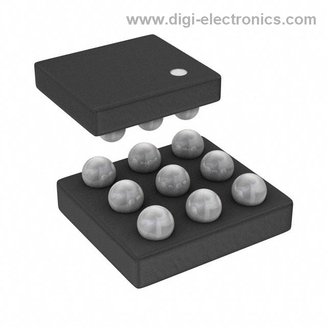
The AD5398BCBZ-REEL7, engineered by Analog Devices Inc., represents an advanced solution for precision current sinking, leveraging a single-channel 10-bit DAC architecture. Its integration in a dense 9-ball WLCSP package (1.52 mm x 1.69 mm) supports streamlined layouts in designs where PCB space is a limiting resource. The device operates across a supply range of 2.7 V to 5.5 V, balancing compatibility with portable electronic platforms and industrial modules that may experience wide supply tolerances.
At its core, the DAC architecture incorporates sophisticated linearity correction and noise mitigation mechanisms. The guaranteed monotonic behavior—crucial for actuator control and imaging applications—eliminates stepwise output errors, directly improving the stability and repeatability of motion systems and optical modules. Embedded within the IC, the integrated current sense resistor supports rapid real-time current monitoring without additional component overhead, allowing fine-grained feedback control and facilitating the implementation of closed-loop current regulation schemes. This underpins reliable operation where output current integrity is paramount, such as in laser diode drive circuits or MEMS actuator interfaces.
The device’s ability to sink up to 120 mA extends its application into demanding actuation roles, including piezoelectric element drive and autofocus motor control in consumer imaging systems or programmable current sources in industrial analog output modules. Thanks to its low-noise internal voltage reference, the AD5398BCBZ-REEL7 yields minimized output ripple and drift, further reinforcing its suitability where high resolution and minimal electrical interference are required.
Deploying the DAC in practice reveals distinct advantages in board-level integration. The WLCSP configuration permits direct routing onto critical signal paths, reducing parasitic capacitances and inductances that commonly undermine signal fidelity in high-current designs. Combined with the reduced component count enabled by the on-chip sense resistor, manufacturing complexity and assembly risk are lowered, expediting prototyping cycles and improving final product reliability in mass production environments.
Close attention to layout—minimizing trace lengths and providing robust ground planes—mitigates EMI issues and maximizes the benefit of the device’s inherent low-noise performance, especially in mixed-signal environments. When applied within actuator feedback loops, the DAC’s precision enables smoother, faster settling with minimal overshoot, which has been validated across diverse industrial use cases.
It is critical to recognize that the AD5398BCBZ-REEL7 bridges the gap between compact form factor and robust current control, a balance not readily achieved with discrete implementations. The combination of monotonicity, integrated sensing, and reference stability positions it as a high-value choice for engineers optimizing signal integrity and functional density. Incorporating such devices into system designs expands the range of achievable performance in compact, current-driven applications, validating its strategic role in next-generation automation and imaging products.
Key features of the AD5398BCBZ-REEL7
The AD5398BCBZ-REEL7’s design reflects advanced integration for applications demanding precision current regulation with strict power requirements. At its core, the device implements a digitally controlled current sink architecture capable of accurate drive outputs up to 120 mA. This output range is particularly advantageous for micro-actuator arrays, laser drivers, and MEMS-based mechanisms, where consistent current translates directly to predictable motion or emission profiles.
The 10-bit digital resolution significantly refines operational granularity, supporting incremental control across 1024 steps. Such precision is instrumental in systems necessitating fine-tuned positioning—examples include camera autofocus actuators and piezoelectric transducers—where sub-milliamp adjustments mitigate overshoot and resonance risks, improving both dynamic response and service life.
Direct integration of a sense resistor is a meaningful enhancement, as it eliminates the errors and assembly complexity associated with external components. Closed-loop current regulation exploits real-time feedback from this internal resistor, ensuring that programmed sink levels remain tightly bounded across temperature and voltage variations. This approach also streamlines EMI management, since board-level routing can be simplified, reducing susceptibility to parasitic coupling common in high-density layouts.
Operating across a single-supply voltage window of 2.7 V to 5.5 V, the IC offers notable deployment versatility. This parameter enables seamless adaptation to both battery-powered mobile platforms and conventional logic rails in fixed installations. It is typical for such current sinks to be deployed in sensor nodes or medical instrumentation, where footprint and efficiency take precedence.
The I²C-compatible serial interface, with support for up to 400 kHz transaction rates and multiple selectable addresses, facilitates flexible system-level communication. Modular integration into processor-managed architectures, ranging from ARM-based controllers to FPGA-driven environments, is commonplace. Efficient register mapping enables rapid updates and multi-channel synchronization, demonstrated in tunable optics and automated test equipment.
Monotonicity, guaranteed across the entire range of digital input codes, is essential in closed-loop control scenarios. Positioning feedback systems and feedback-driven illumination drivers benefit when every digital increment results in a corresponding, non-retrograde output change, eliminating jitter and step reversal failures that could compromise precise feedback loops.
Ultralow typical quiescent current in power-down mode—approximately 0.5 µA—addresses modern requirements for energy conservation without sacrificing readiness or responsiveness. This characteristic is leveraged in wearable medical sensors and wireless actuator nodes, where extended operating intervals between battery service events are critical.
A built-in power-on reset ensures the output defaults to zero volts upon startup, reinforcing system safety protocols and deterministic initialization, particularly in mission-critical embedded control systems.
Package miniaturization, realized via 9-WLCSP and 8-lead LFCSP variants, supports high-density PCB layouts where interconnect routing efficiency and opto-electronic coupling must be maximized within space-constrained modules. Implementation experience suggests that such compact form factors lower parasitic effects, improve mechanical robustness in vibration-prone conditions, and simplify automated assembly processes.
Collectively, the AD5398BCBZ-REEL7 sets a reference point for compact, low-power current sink solutions that do not compromise on resolution or reliability. The nuanced integration of the sense resistor, coupled with monotonic behavior and efficient interface protocols, creates a pathway for robust performance in precision-driven systems, even under thermal or supply voltage stress. The holistic attention to packaging and quiescent current parameters allows deployment in domains previously restricted by physical and energy constraints, implying potential for wider adoption in next-generation portable and miniaturized control platforms.
Operating principles and internal architecture of the AD5398BCBZ-REEL7
The operational framework of the AD5398BCBZ-REEL7 centers on precise digital-to-analog current translation through a 10-bit input received via the I²C interface. The device’s internal digital-to-analog converter is streamlined for direct communication with microcontrollers, enabling dynamic adjustment of current drive based on real-time system demands. Critical to this operation is a dedicated current sense pathway, constructed around matched and integrated resistive elements, which stabilize output current by forming a feedback loop that compensates for external variation, including temperature fluctuations and load impedance changes. This architecture not only suppresses drift but also sustains linear performance, particularly critical for closed-loop actuator applications where precision motion control is necessary and environmental shifts are routine.
The analog drive stage is optimized for inductive loads with low resistance, such as miniaturized voice coil mechanisms in optical modules or precision solenoids in industrial positioning systems. By integrating resistor pairs with tight process matching, the device achieves minimal gain error and sustains transfer function integrity throughout its -40°C to +85°C operational envelope. Such biasing stability is essential in mobile imaging modules, where autofocus accuracy directly impacts system calibration and user-perceived quality. The direct current output eliminates intermediary drive stages, trimming latency and simplifying PCB layout for dense, multi-axis assemblies.
An efficient power management subsystem is embedded, allowing transitions to a low-power state with negligible leakage when the actuator interface is inactive. This feature is inherently advantageous in extended duty-cycle platforms—where current conservation translates directly to reduced thermal footprint and extended operational range. Such architecture supports designs for compact robotics and battery-optimized industrial sensors, where system longevity is strongly coupled to current drain profiles.
Output-stage protection has been thoughtfully integrated, with an emphasis on safeguarding against voltage excursions caused by inductive kickback or anomalous disconnects. The inclusion of a robust clamping diode at the output prevents charge accumulation and potential latch-up, ensuring endurance against both sporadic transients and repetitive high-frequency drive signals typical in modulated actuator systems. This strategic integration provides immunity to failure modes that could otherwise propagate downstream, enhancing system reliability without recourse to bulky external protection components.
Careful architecture choices—single-interface programmability, matched resistive controls, and granular power management—collectively sharpen deployment flexibility across mass-market mobile modules and high-precision industrial subsystems. Observed application outcomes consistently demonstrate that leveraging a digitally-controlled proportional current sink, together with intrinsic thermal and transient protections, shortens development cycles and lowers field maintenance costs. A measured perspective reveals that such devices not only satisfy functional benchmarks but redefine reliability expectations in densely integrated, mission-focused electronics, supporting scaling from prototype through volume production without legacy drift or interface incompatibility.
Application scenarios for the AD5398BCBZ-REEL7
The AD5398BCBZ-REEL7 is architected as a highly integrated 8-bit, single-channel, programmable current source, optimized to address the rigorous requirements of both advanced imaging and industrial automation systems. Its primary functional strength lies in precise, adjustable current output, which underpins its suitability for fine-grained actuator and electromotive applications.
At the fundamental level, the device employs a serial digital interface (I²C) for streamlined integration with microcontrollers or DSPs. This digital interface eliminates complex analog control circuits, allowing deterministic, low-latency configuration for real-time current modulation. Internally, a high-resolution R-2R DAC architecture ensures monotonic current stepping, which is essential for eliminating mechanical jitter in sensitive actuation mechanisms such as voice coil motors or Peltier thermal elements.
In modern imaging systems, miniaturization and efficiency are continuous challenges. The AD5398BCBZ-REEL7 enables compact lens actuators to achieve rapid position settling, directly impacting autofocus speed and reliability. Its low quiescent current extends battery life, a non-negotiable requirement in portable devices where every milliwatt affects run time and thermal headroom. The device’s fine current granularity supports emergent high-resolution imaging demands, ensuring seamless operation in tiny lens movement increments for optical stabilization, iris tuning, and adaptive filter deployment. The resulting improvement in precision translates into sharper images and enhanced control over optical parameters, particularly beneficial in advanced multi-sensor camera modules.
The device’s form factor and minimal external component dependence enable its control loop to be tightly co-located with the actuated element, reducing parasitic losses and electromagnetic interference. Products such as smartphone cameras, high-zoom surveillance modules, and body-worn recorders leverage this attribute to maintain image capture fidelity in dynamic or constrained environments.
For industrial automation, the device’s programmable current control directly translates to accurate manipulation of thermal actuators, linear actuators, and solenoid-based switching assemblies. The deterministic I²C interface is particularly beneficial for automation architectures where command stacking and quick reconfiguration are mandatory, such as in automated optical inspection rigs or reconfigurable factory cells. The output’s low drift response ensures that temperature-sensitive processes like Peltier-based thermal cycling can be tightly controlled over long operational windows, crucial for semiconductor test handlers and precision incubation chambers.
Industrial reliability is further reinforced through the AD5398BCBZ-REEL7’s robust protection features and predictable transient response; these characteristics help prevent overdrive conditions and extend the service life of mechanical components even with high-frequency switching cycles. In distributed control topologies, the device’s ability to occupy minimal PCB real estate while providing high-precision analog current output makes it an ideal node in dense analog current loop architectures. This is particularly valuable in sensor fusion hubs, actuator networks, and modular test platforms, where channel density and noise immunity are primary concerns.
A recurring practical insight is that the device’s digital programmability simplifies not only initial configuration but also real-time calibration, enabling adaptive systems that modify actuator behavior in situ based on environmental feedback. This adaptability distinguishes it from purely analog sources, granting greater system robustness in the face of aging, temperature drift, or mechanical wear. Additionally, the explicit control granularity afforded by the device supports custom motion profiles or thermal ramps, enhancing application-specific performance in environments where one-size-fits-all actuation is unviable.
Ultimately, the AD5398BCBZ-REEL7’s integration of digital intelligence with stable analog actuation addresses the practical engineering challenges encountered in applications demanding high spatial or thermal precision within constrained energy and volume budgets. Such capabilities enable next-generation optics, thermal regulation, and automation platforms to deliver consistent, precise operation across a broad spectrum of real-world deployment contexts.
Integration and layout considerations for the AD5398BCBZ-REEL7
Integration and layout optimization of the AD5398BCBZ-REEL7 begins with a rigorous approach to supply and ground domain management. The device's architecture features separated analog (AGND) and digital (DGND) grounds, demanding careful layout discipline. Connecting AGND and DGND at a single, low-impedance node placed immediately underneath or beside the IC dramatically reduces the risk of ground potential differences that can introduce subtle but significant measurement errors, particularly in precision current sink configurations. Overlapping ground planes can be highly effective on multilayer PCBs, but the connection strategy must avoid unintended coupling, as even short loops or parasitic traces can propagate high-frequency interference.
Power distribution network design must aim for minimal resistive and inductive losses. Short, wide traces sharply reduce IR drops and loop area, directly improving regulation margins. In current control applications, trace resistance directly translates to wasted compliance voltage; excessive series resistance constrains maximum output current as demonstrated when operating with a 3.6 V rail. Under such conditions, even minor increases in return trace resistance can push the total load plus wiring beyond the 600 mV compliance limit, triggering early current limiting or control instability. Experience shows that using 50–100 mil wide traces for both supply and return within a few centimeters of the device strikes an optimal balance of manufacturability and electrical performance, with reduced risk of hotspots or oscillatory behavior at high slew rates.
Capacitive decoupling is not optional. High-frequency supply noise can couple into the analog reference or output stages, degrading settle time or causing sporadic output shifts. Deploying a local 0.1 µF X7R ceramic capacitor within millimeters of the device supply greatly suppresses radio-frequency artifacts, while a parallel 10 µF tantalum bulk capacitor dampens lower-frequency load transients. Direct via stitching to a solid ground plane beneath the capacitors and device is essential. On boards with more demanding environmental conditions or stringent EMC requirements, supplementing with an additional ferrite bead in series with the supply line further attenuates conducted noise above 100 MHz without impacting dynamic response.
Thermal dissipation cannot be overlooked when targeting higher sink currents, notably in WLCSP or LFCSP footprints with exposed thermal pads. Soldering the pad directly to the ground plane enables efficient lateral and vertical heat spreading—crucial for maintaining device reliability and stable operation under sustained load. Board stackups that sandwich internal ground planes directly under the device allow efficient heat evacuation and also enhance analog noise immunity, especially in compact layouts subject to strong digital or RF field coupling.
Practical experience reveals that implementing continuous ground pours under and around the device, and separating sensitive analog traces from high-speed digital or PWM control lines, consistently yields best-in-class output stability and limits noise injection. Further, the sequencing of power-up events—ensuring analog rails settle before digital logic is enabled—can mitigate start-up anomalies in high-integrity analog systems.
Applied with this layered strategy, the integration of the AD5398BCBZ-REEL7 supports robust, low-noise current regulation, even in mixed-signal or thermally stressed environments. From underlying grounding topology through power integrity and thermal routing, disciplined layout yields consistently superior performance and unlocks the full accuracy potential of the device.
Interface and communication details for the AD5398BCBZ-REEL7
The AD5398BCBZ-REEL7 employs an I²C-compatible, two-wire serial interface designed for direct integration into diverse embedded control architectures. This interface leverages standard I²C signaling, operating across a 7-bit address space (0x18 to 0x1F), allowing for straightforward device stacking and address selection by configuring less significant bits at the hardware or firmware level. The device fully supports both master-initiated read and write sequences, making it adaptable for complex communication topologies while maintaining backward compatibility with legacy I²C system masters. Bus operation at frequencies up to 400 kHz achieves a critical balance between data throughput and robust noise resilience on longer PCB traces or through multi-drop configurations.
Communication protocol is optimized for efficiency. Each 10-bit digital-to-analog control word is formatted across two consecutive data bytes, packed to include not only the voltage-setting data but also the power-down state, enabling in-band management of both conversion and power control within a single write cycle. This multiplexed data structure minimizes I²C bus contention and facilitates rapid context switches between active and low-power modes in dynamic operational environments.
Upon successful transaction completion, the DAC register latches new data immediately, leading to minimal analog output latency—an essential attribute for real-time feedback and servo control applications where phase lag or delayed actuation can compromise closed-loop system stability. Importantly, the integration of power-on reset circuitry guarantees the DAC initializes to a defined state after power cycling. This deterministic startup behavior prevents inadvertent analog output glitches that might otherwise propagate destabilizing signals into sensitive loads or downstream analog subsystems.
The device’s software-controlled power-down function establishes fine control over system power budgets. By embedding power-down flags in the same I²C transaction as the DAC setting, rapid mode arbitration enables highly granular management of peripheral power at the board level, essential in battery-operated platforms such as wearables, instrumentation, or portable medical devices.
Practical deployment highlights several nuances critical to reliable performance. Pull-up resistors on the I²C lines must be carefully dimensioned, balancing rise-time requirements against bus loading constraints to maintain integrity under varying line capacitance scenarios. In multi-device chains, address assignment planning prevents cross-talk and ensures each device is uniquely addressable without risk of conflicting responses. Additionally, proper sequencing of power-down commands in system firmware prevents analog drift or spurious output states during transitions, further safeguarding application stability.
One core insight emerges: the deterministic and tightly coupled interface and power management scheme of the AD5398BCBZ-REEL7 enables precise, low-latency analog output control while minimizing overall system complexity. This approach not only smooths physical integration but also empowers robust, scalable system-level designs where analog performance and communication reliability are equally mission-critical.
Potential equivalent/replacement models for the AD5398BCBZ-REEL7
Evaluating equivalent or alternative models for the AD5398BCBZ-REEL7 requires a comprehensive understanding of both its core technical attributes and nuanced operational demands. This DAC is characterized by high-current drive capability, monotonic 10-bit resolution, and an integrated sense resistor, bundled with an I²C-compatible serial interface. Such specifications distinctly position the device for precise current control applications, typically in compact embedded systems where board space is at a premium and thermal performance must be tightly managed.
Replacing the AD5398BCBZ-REEL7 involves identifying alternatives with compatible electrical profiles. Core criteria must include monotonicity across the entire code range for predictable analog output and avoidance of non-linear artifacts, especially in closed-loop systems. Minimum 10-bit resolution is required to resolve fine current steps, which is critical for applications needing granular current or light intensity adjustments, such as driving configurable laser diodes or controlling analog actuators.
Attention must be given to maximum output current and compliance voltage: alternatives must not only reach the required current without saturation but also maintain specified linearity and dynamic performance within the voltage constraints of the load. Integrated sense resistors are essential for streamlined PCB layouts and simplified current measurement and feedback; their presence reduces external parasitic effects and design complexity. Noise characteristics, often overlooked, become especially relevant in precision analog control—low output noise ensures stable operation in sensitive analog front ends or optical modulation circuits.
When surveying replacements from Analog Devices and other manufacturers, device package compatibility also influences the feasibility of drop-in substitution, as mechanical mismatch can lead to redesign costs and qualification delays. Interface conventions such as I²C or SMBus must be matched to existing code bases and firmware architectures to avoid significant software rework.
A practical evaluation often involves setting up test harnesses for alternative DAC candidates under representative load conditions. Real-world trials reveal thermal behavior under sustained operation and uncover subtle pin or timing differences that may not be fully detailed in datasheets. Systematic stress testing of monotonicity and output accuracy—using automated calibration routines with known benchmarks—can surface outlier behaviors under temperature drift or supply variation.
Advanced selection leverages cross-manufacturer databases for parametric comparison, favoring devices with field-proven reliability metrics documented in automotive or industrial deployments. A valuable insight is that marginal improvements in output noise or compliance margins can simplify system-wide EMC and qualification requirements, producing indirect savings throughout the lifecycle of the final product.
Efficient substitute screening benefits from modular design approach—isolating the current-generation DAC on a breakout PCB allows for rapid evaluation of fit and function with candidates. Preference should be given to devices with accessible reference designs, comprehensive support documentation, and responsive technical channels, as the integration phase frequently exposes edge-case anomalies.
Ultimately, a rigorous and structured method for alternate selection, encompassing direct electrical equivalence and broader application fit, mitigates both technical and logistical risk. Experience with iterative testing in live environments discerns the subtle interplay of DAC characteristics and system stability, refining the pathway to robust design choices.
Conclusion
The AD5398BCBZ-REEL7 integrates advanced digital-to-analog conversion with a high-current output stage, streamlining the interface between logic-level controllers and demanding electronics such as actuators and variable drivers. At its core, the device leverages a 10-bit DAC architecture, enabling fine granularity in output adjustment—essential for precise positioning or drive modulation in imaging elements and industrial mechanisms. The robust current capability of the output stage meets requirements for direct control of low-impedance loads, reducing external component count and minimizing board area.
Noise performance is engineered for stable operation, supporting sensitive analog subsystems within compact form factors. Low-noise characteristics mitigate electromagnetic interference risk and ensure clean transitions during rapid setpoint changes, which is critical for reproducing smooth lens shifts or vibration-free robotic joint movements. The I²C interface simplifies connectivity, allowing for efficient multi-device communication and reducing firmware complexity. This eases integration into platforms where space and CPU resources are constrained, while also enabling precise command timing for synchronized multi-axis control.
Beyond basic functionality, the AD5398BCBZ-REEL7 embodies a design philosophy that prioritizes versatility under stringent environmental and operational constraints. Its electrical protection schemes safeguard downstream loads during transient conditions, such as startup or fault states, enhancing overall system reliability. In practical deployments, direct drive capability eliminates the need for buffer amplifiers, which not only streamlines the signal chain but also reduces thermal dissipation and latency in feedback-controlled systems.
When deployed in focus and zoom actuators of camera modules, the device supports rapid lens adjustment cycles with minimal lag and consistent repeatability. In industrial setups, it enables high-precision control of solenoid valves or proportional motors, responding accurately to algorithmic setpoints without calibration drift. Modular scalability is another key insight: by assigning addressable I²C instances, engineers create distributed actuator networks with simplified wiring and centralized supervisory control.
The AD5398BCBZ-REEL7 thus represents the convergence of integration, reliability, and scalability in modern electromechanical system design. Its operational metrics reflect a nuanced understanding of real-world constraints, optimizing both component density and application-level performance. These attributes distinguish it as a foundational solution for building next-generation platforms where analog drive precision and digital ease converge.